

RF circuit component and RF circuit
- Summary
- Abstract
- Description
- Claims
- Application Information
AI Technical Summary
Benefits of technology
Problems solved by technology
Method used
Image

Examples
embodiment 1
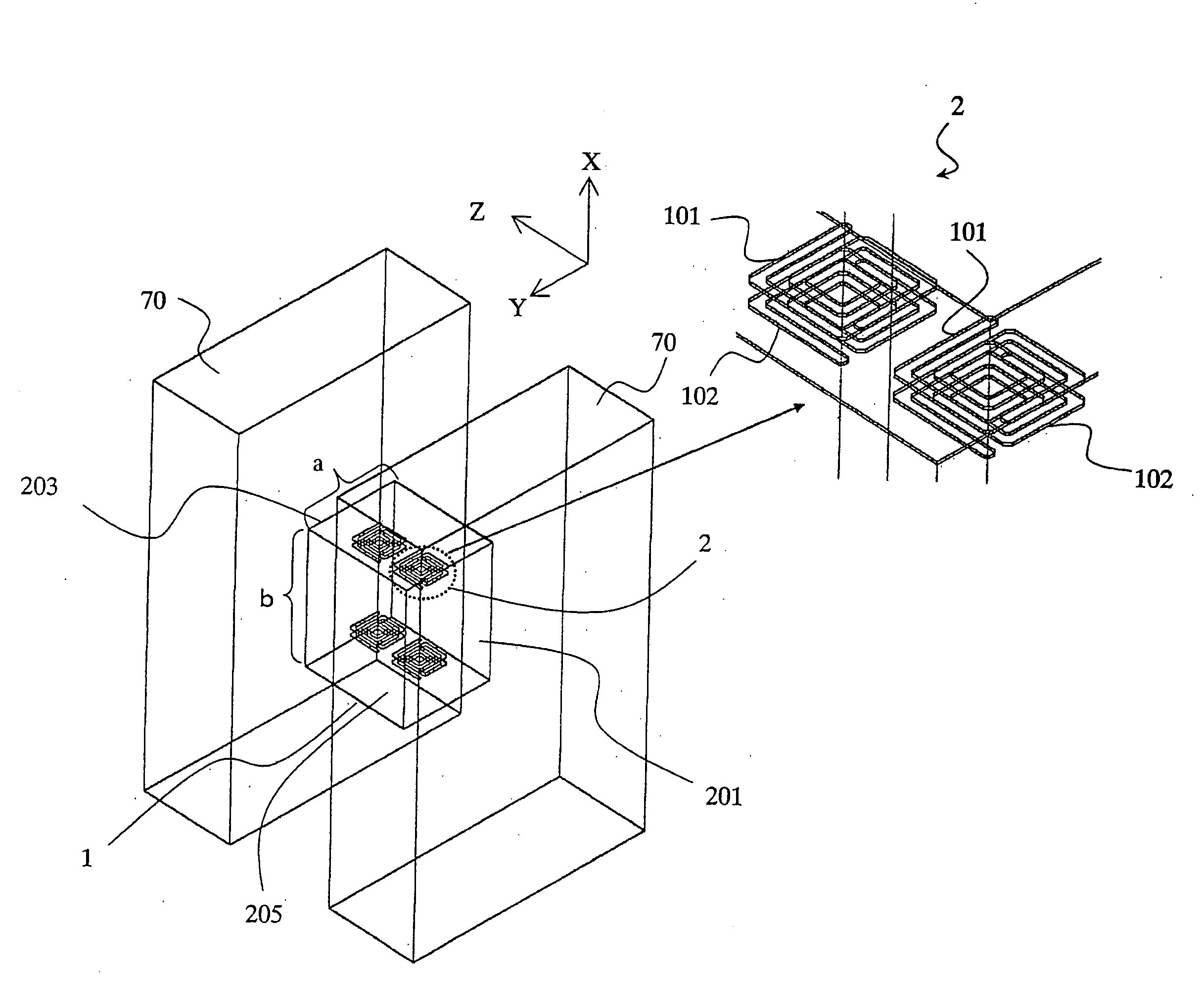
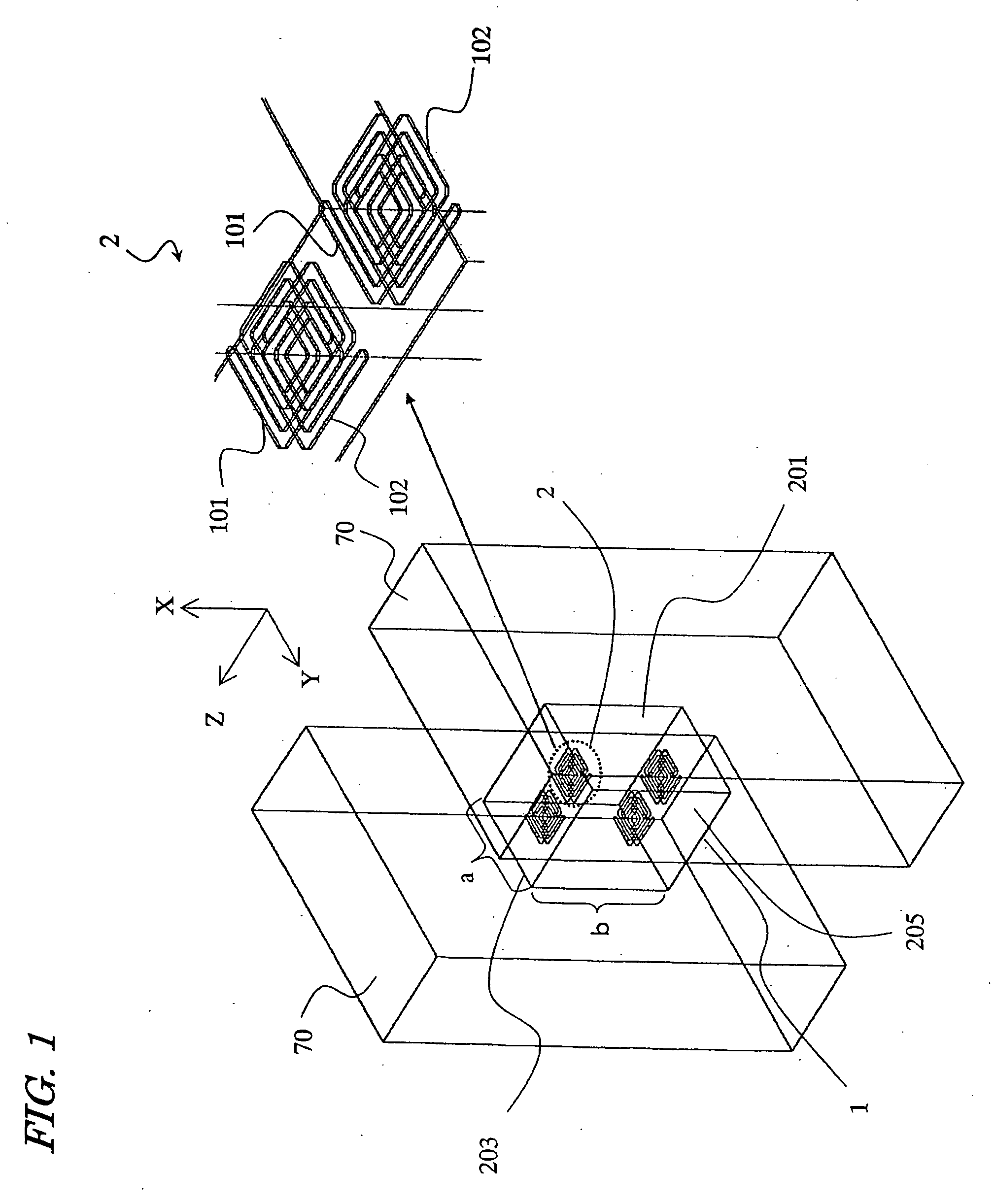
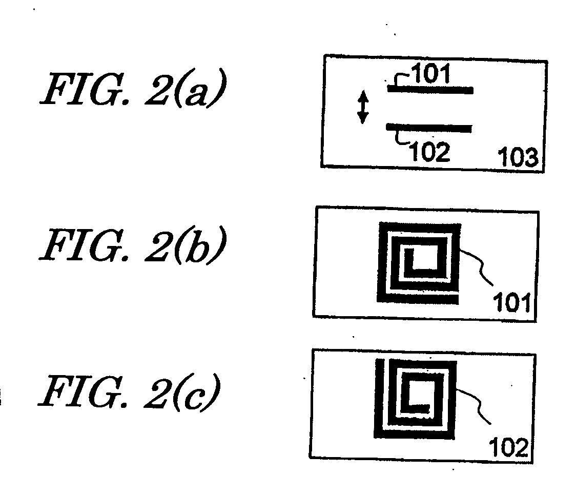
[0063] Hereinafter, a first specific preferred embodiment of an RF circuit component according to the present invention will be described with reference to FIG. 1. The RF circuit component of this preferred embodiment shown in FIG. 1 includes a waveguide 1 and a plurality of resonators 2, which are arranged inside the waveguide 1. Input / output portions 70 are arranged on both sides of the waveguide 1. As will be described in detail later, each resonator 2 includes at least one patterned conductor layer (e.g., conductor lines 101, 102). By adjusting the shape and arrangement of this conductor layer, resonances can be caused at lower frequencies than the “cutoff frequency fc” that is defined by the waveguide 1, and electromagnetic waves with lower frequencies than the cutoff frequency fc can pass the waveguide 1. FIG. 1 also illustrates some resonators 2 on a larger scale, where the conductor lines 101 and 102 are illustrated as if those lines were transparent such that it can be seen...
example 1
[0107] Hereinafter, Examples Nos. 1-1 through 1-12 of an RF circuit component according to the present invention will be described with reference to FIG. 8.
[0108]FIG. 8 illustrates a basic configuration for Examples Nos. 1-1 through 1-11. FIG. 8(a) is a transparent perspective view of this example and FIG. 8(b) is a side view thereof.
[0109] As shown in FIG. 8, the waveguide of each example includes two input / output portions 7 and a constricted portion 8 sandwiched between the input / output portions 7. The waveguide is made of a resin material with a dielectric constant of 10.2 and is designed such that the cross section of the constricted portion 8 at the center is smaller than the cross section of the input / output portions 7. The constricted portion 8 has a vertical size of a mm and a horizontal size of b mm, while the input / output portions 7 have a vertical size of A mm and a horizontal size of B mm. In Example No. 1-1, A was set to 25 mm and B was set to 32 mm.
[0110] In this ca...
embodiment 2
[0139] Hereinafter, a second preferred embodiment of an RF circuit component according to the present invention will be described. The RF circuit component of this preferred embodiment is a slot antenna.
[0140] First, referring to FIG. 11, illustrated are a perspective view showing the structure of an RF circuit component according to this second preferred embodiment in FIG. 11(a) and a cross-sectional view thereof as viewed on a plane indicated by the dotted line in FIG. 11(b), respectively. In FIG. 11, each component, which is the same as, or corresponds to, its counterpart shown in FIG. 14, is identified by the same reference numeral.
[0141] Just like the slot antenna shown in FIG. 14, the slot antenna shown in FIG. 11 also includes a dielectric substrate 21, which includes a grounded conductor layer 23 on the back surface thereof. A strip-shaped slot 24 is cut through the center of the grounded conductor layer 23. On the surface of the dielectric substrate 21, a signal conductor...
PUM
 Abstract
Description
Claims
Application Information