Dielectric layer, semiconductor memory device including the dielectric layer, and methods of manufacturing the dielectric layer and the semiconductor memory device

Active Publication Date: 2019-10-31
KOREA INST OF SCI & TECH
View PDF0 Cites 2 Cited by
  • Summary
  • Abstract
  • Description
  • Claims
  • Application Information

AI Technical Summary

Benefits of technology

[0008]The present invention provides a dielectric layer capable of ensuring low leakage current characteristics of a capacitor and of increasing a dielectric constant, a semiconductor memory d

Problems solved by technology

However, the capacitor is reduced in size to increase an integration density of the device, and the capacitance value proportional to an area is unavoidably reduced due to the reduced capacitor size.
Therefore, when a material having a high dielectric constant is used, an increase in a layer thickness is unavoidable to reduce a leakage current.
As a design rule of 20 nm or less is applied to DRAM devices, a limitati

Method used


Image

  • Dielectric layer, semiconductor memory device including the dielectric layer, and methods of manufacturing the dielectric layer and the semiconductor memory device
  • Dielectric layer, semiconductor memory device including the dielectric layer, and methods of manufacturing the dielectric layer and the semiconductor memory device
  • Dielectric layer, semiconductor memory device including the dielectric layer, and methods of manufacturing the dielectric layer and the semiconductor memory device

Examples


Example

[0035]Hereinafter, the present invention will be described in detail by explaining embodiments of the invention with reference to the attached drawings. The invention may, however, be embodied in many different forms and should not be construed as being limited to the embodiments set forth herein; rather, these embodiments are provided so that this disclosure will be thorough and complete, and will fully convey the concept of the invention to one of ordinary skill in the art. In the drawings, the sizes of at least some elements are exaggerated or reduced for convenience of explanation, and like reference numerals denote like elements.

[0036]As used herein, the term “room temperature” refers to the temperature of natural indoor air which is not artificially heated or cooled, and may include, for example, a temperature range from 0° C. to 50° C.

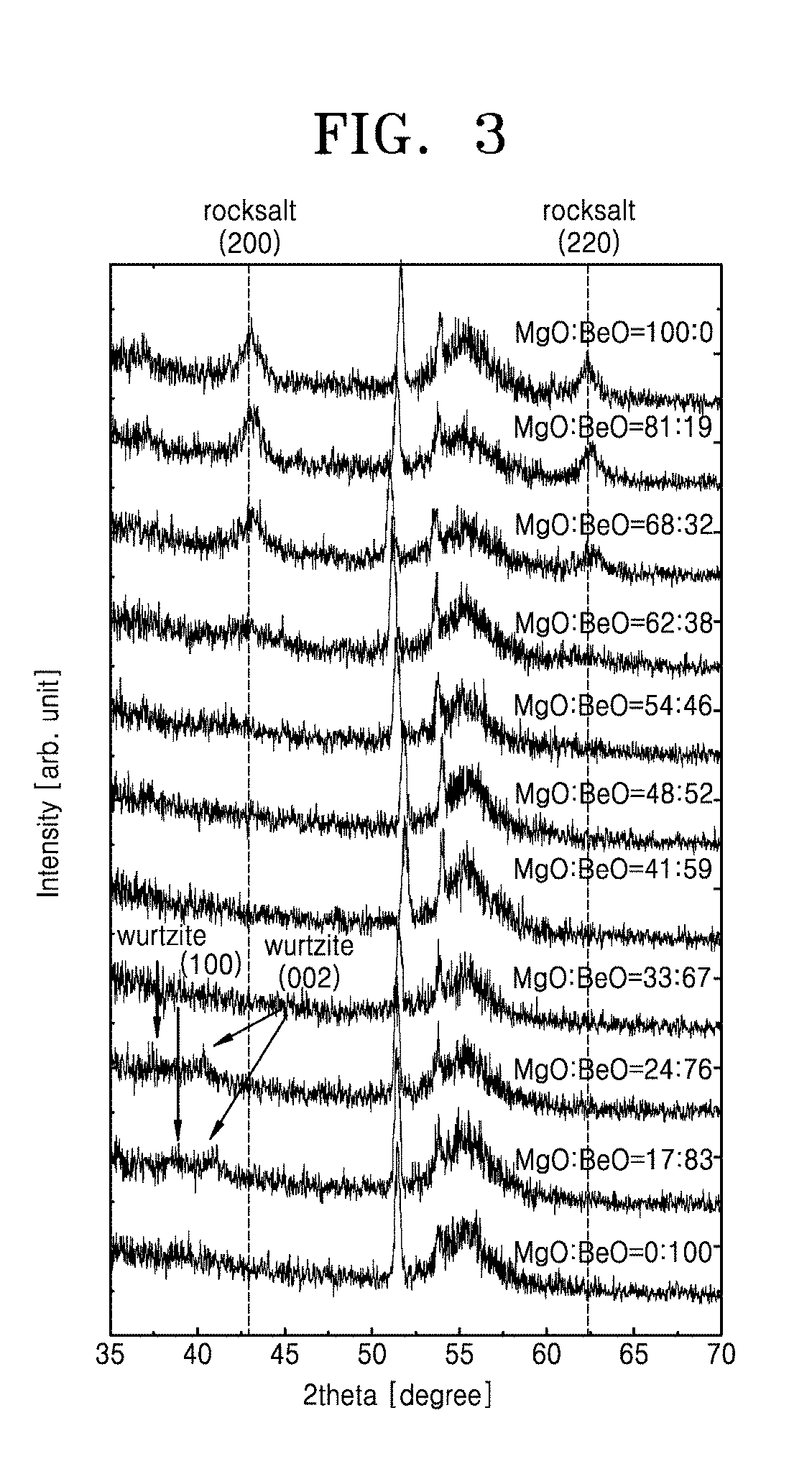
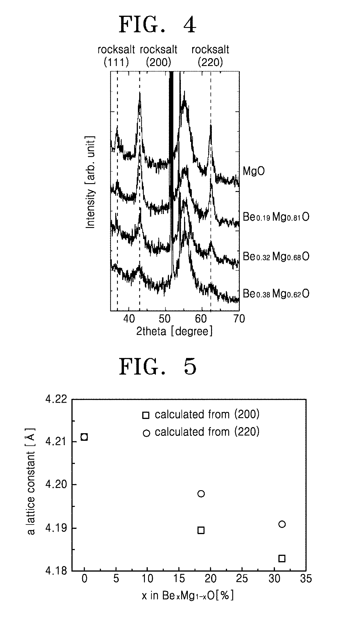
[0037]In a rocksalt structure described below, cations and anions may have the same coordination number of 6 and a cation-anion radius ratio ma...


PUM


Abstract

Provided is a dielectric layer that has a rock salt structure in a room temperature stable phase. The dielectric layer is made of a compound having a chemical formula of BexM1-xO, where M includes one of alkaline earth metals and x has a value greater than 0 and less than 0.5.

Description

CROSS-REFERENCE TO RELATED PATENT APPLICATION[0001]This application claims the benefit of Korean Patent Application No. 10-2018-0047915, filed on Apr. 25, 2018, in the Korean Intellectual Property Office, the disclosure of which is incorporated herein in its entirety by reference.BACKGROUND1. Field[0002]The present invention relates to a dielectric layer, a semiconductor memory device including the dielectric layer, and methods of manufacturing the dielectric layer and the semiconductor memory device and, more particularly, to a dielectric layer having a high dielectric constant and a large band gap, a semiconductor memory device including the dielectric layer, and methods of manufacturing the dielectric layer and the semiconductor memory device.2. Description of the Related Art[0003]Currently, integration densities of semiconductor devices exponentially increase along with rapid development of semiconductor industries. Ultra large-scale integration (ULSI) dynamic random-access memo...

Claims


Application Information

Patent Timeline
IPC IPC(8): H01L23/532H01L49/02H01L27/108
CPCH01L28/60H01L27/10844H01L23/5329H01L28/40H10B12/30H01L21/0228H01L21/02194H01L28/90H10B12/03H01L21/762H10B12/01C01F3/02H10B12/00
Inventor KIM, SEONG KEUNLEE, WOO CHULKIM, SANG TAESONG, HYUN CHEOLBAEK, SEUNG HYUBCHOI, JI WONKIM, JIN SANGKANG, CHONG YUNBIELAWSKI, CHRISTOPHER W.YUM, JUNG HWANLARSEN, ERIC S.
Owner KOREA INST OF SCI & TECH
Why Eureka
Try Eureka