Fabrication method of a semiconductor device and a semiconductor device

Inactive Publication Date: 2010-02-04
TOKYO ELECTRON LTD
View PDF9 Cites 7 Cited by
  • Summary
  • Abstract
  • Description
  • Claims
  • Application Information

AI Technical Summary

Benefits of technology

[0027]According to one aspect of the invention, an increase in an effective dielectric constant of the internal insulation films locating between an upper layer wiring and a lower layer wiring is suppressed, so that the advantage on a fluorine-doped carbon film, having a low dielectric constant, is applied to a semiconductor device having a fluorine-doped carbon film that is used as an internal insulation film. In a conventional case, a capping film such as a SiCN film having a relatively hig

Problems solved by technology

For example, compared to a film that includes silicon as the dominant element, there are disadvantages of the fluorine-doped

Method used


Image

  • Fabrication method of a semiconductor device and a semiconductor device
  • Fabrication method of a semiconductor device and a semiconductor device
  • Fabrication method of a semiconductor device and a semiconductor device

Examples


first embodiment

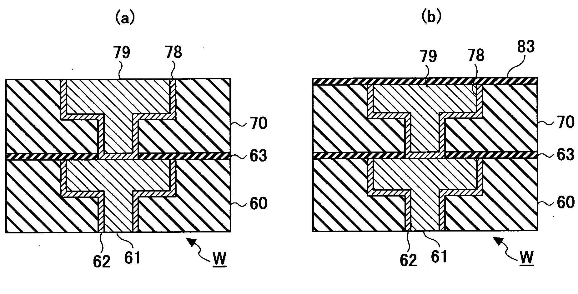
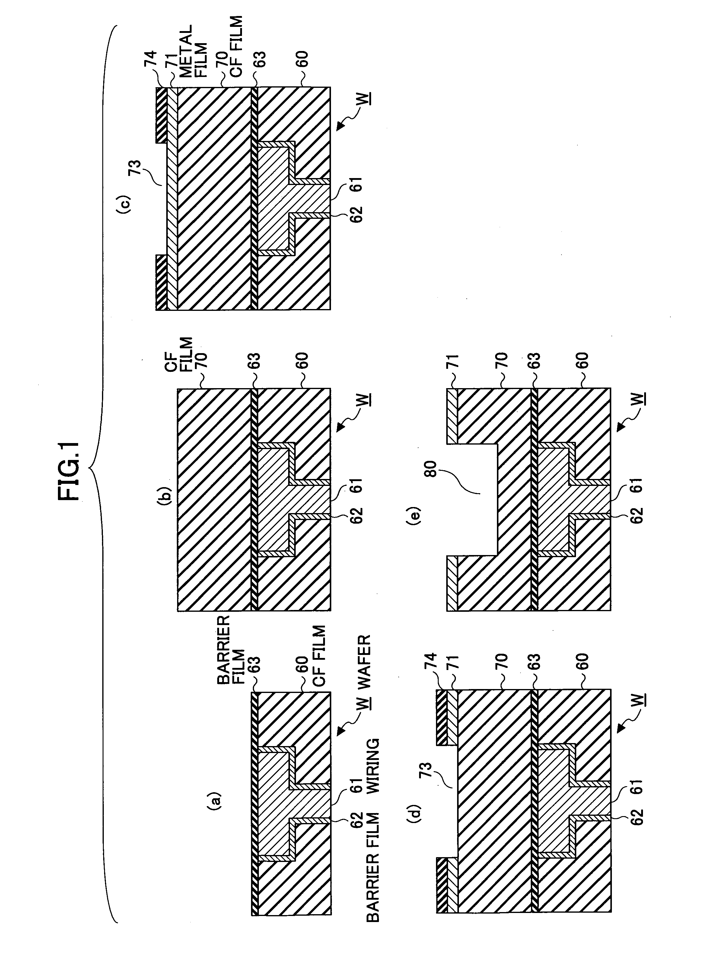
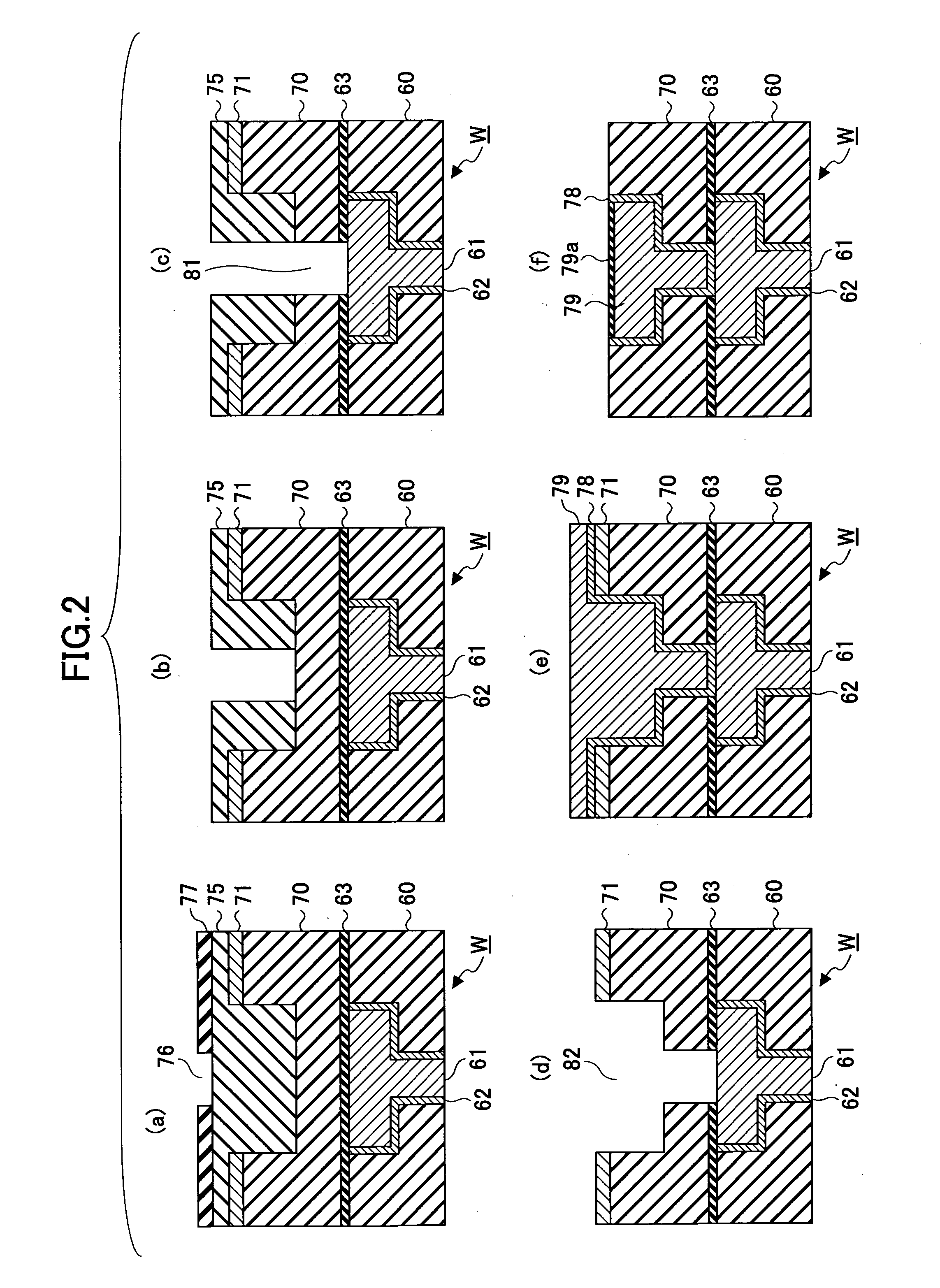
[0036]With reference to FIG. 1, an embodiment of a fabrication process of the semiconductor device related to the present invention is explained. FIG. 1(a) shows a number n (lower side) circuit layer formed on a wafer W which is a substrate. The circuit layer includes that a metal wiring 61 made of such as Cu is supplied to fill in a fluorine-doped carbon film (written as a CF film in the following) 60 that is an internal insulation film. There is a barrier metal film 62 between the CF film 60 and the wiring 61 for preventing the diffusion of the wiring 61 material into the CF film 60, where the barrier metal film 62 is formed by a multilayer that is formed from the bottom side (CF film 60 side) in order of a titanium nitride (TIN) film and a tantalum (Ta) film. Further, a barrier film 63 made of SiC or the like is formed on this circuit layer for preventing metal diffusion into the CF film 70, which is the number (n+1) layer from the wiring 61. In the following explanation, the num...

embodiment

Experimental Example 1

[0059]When a silicon compound related film, for example a SiCN film was used as the above described capping layer, it remained as part of an internal insulation film. An effect on a SiCN film in an internal insulation film for a dielectric constant was investigated in the following. In the experiment, different structures were formed. The thicknesses of CF films were varied from 100 nm to 375 nm by 25 nm steps, and each of the films was formed on a 20 nm thick SiCN film. Another 20 nm thick SiCN film was formed on a CF film to sandwich the CF film. The dielectric constants of the structured films were measured by using the mercury probe system.

Experimental Result

[0060]The measurement results are shown in FIG. 6. It is seen that a dielectric constant of the structured internal insulation film increases with decreasing the film thickness of a CF film. This suggests that when the whole thickness of the internal insulation film decreases, the dielectric constant of...

experimental example 2

Experimental Example 2-1

[0061]A CF film is formed on a wafer W by using the film formation equipment 10. C5F8 gas was used as source gas having a straight chain structure, and a Ti film was formed on the CE film by using a sputtering method. A thermal treatment was performed at 400° C. for 60 minutes in a vacuum atmosphere.


PUM


Abstract

A method for fabricating a semiconductor device includes the steps of (a) forming a plasma of a gas having carbon and fluorine, and forming an internal insulation film provided with a fluorine-doped carbon film formed on a substrate using the plasma; (b) forming a metal film on the internal insulation film; (c) etching the metal film according to a pattern to form a hard mask; (d) forming a concave part in the fluorine-doped carbon film by etching the fluorine-doped carbon film using the hard mask; (e) forming a film formation of a wiring material on the substrate for filling the concave part with the wiring material; (f) removing an excess part of the wiring material and the hard mask on the fluorine-doped carbon film for exposing a surface of the fluorine-doped carbon film; and (g) removing an oxide formed on the surface of the fluorine-doped film.

Description

TECHNICAL FIELD[0001]The present invention relates to a fabrication method for a semiconductor device including an internal insulation layer of a fluorine-doped carbon film and a semiconductor device including the fluorine-doped carbon film.BACKGROUND ART[0002]Multilayer wiring structures are used to increase the integration of semiconductor devices.[0003]Although multilayer wiring structures are applied to increase the integration of semiconductor devices, it becomes easier for signals to transmit through internal insulation layers as the signal frequencies increase. Therefore, it is required to reduce the dielectric constants of the internal insulation layers for further increasing the operational speeds of semiconductor devices. In general, a SiO2 film (silicon dioxide film) is used, and the relative dielectric constant (written as the dielectric constant in the following) of SiO2 is 4.0 and as lesser dielectric constant material, a SiOF film with a dielectric constant of 3.6 is ...

Claims


Application Information

Patent Timeline
IPC IPC(8): H01L23/522H01L21/768
CPCC23C16/26H01L21/02074H01L21/0212H01L21/02274Y10S438/951H01L21/31144H01L21/3127H01L21/76808H01L21/76883H01L21/02304H01L21/28H01L21/768
Inventor KAWAMURA, KOHEINOZAWA, TOSHIHISAMATSUOKA, TAKAAKI
Owner TOKYO ELECTRON LTD
Why Eureka
Try Eureka