Method of making an ultrathin silicon dioxide gate with improved dielectric properties using NH3 nitridation and post-deposition rapid thermal annealing

Inactive Publication Date: 2006-03-28
TAIWAN SEMICON MFG CO LTD
View PDF2 Cites 4 Cited by
  • Summary
  • Abstract
  • Description
  • Claims
  • Application Information

AI Technical Summary

Benefits of technology

[0032]Another embodiment of the invention includes a method of making a semiconductor device having a silicon dioxide based gate with improved dielectric properties including providing the silicon based substrate having active areas defined therein. Heating the silicon based substrate in the presence of wet o

Problems solved by technology

The ultrathin gate dielectric has been emerged as one of the hardest challenges for further device scaling.
No suitable alternative high dielectric constant material and interface layer has been identified with the stability and interface characteristics to serve as a gate dielectric.
For so-call high-K metal oxides, such as HfO2, ZrO2, Ta2O5, TiO2, unfortunately most of these materials have thermal stability issues.
However, annealing causes the further growth of the SiO2 and silicide, which reduces the effectiveness of any high-K materials.
Furthermore, these materials can't endure subsequent high-temperature source/drain and gate activation, which will crystallize the high-K films and thus results in large leakage increase.
It is also not clear if any of these materials are compatible with poly-Si gate due to the chemical reactivity with the poly-Si.
Therefore, the obstacles for high-K material are not only the discovery and development of a new material, but possibly a complete re-engineering of ever more complicated CMOS processing.
However, there still exists some problems including the signific

Method used


Image

  • Method of making an ultrathin silicon dioxide gate with improved dielectric properties using NH3 nitridation and post-deposition rapid thermal annealing
  • Method of making an ultrathin silicon dioxide gate with improved dielectric properties using NH3 nitridation and post-deposition rapid thermal annealing
  • Method of making an ultrathin silicon dioxide gate with improved dielectric properties using NH3 nitridation and post-deposition rapid thermal annealing

Examples


Example

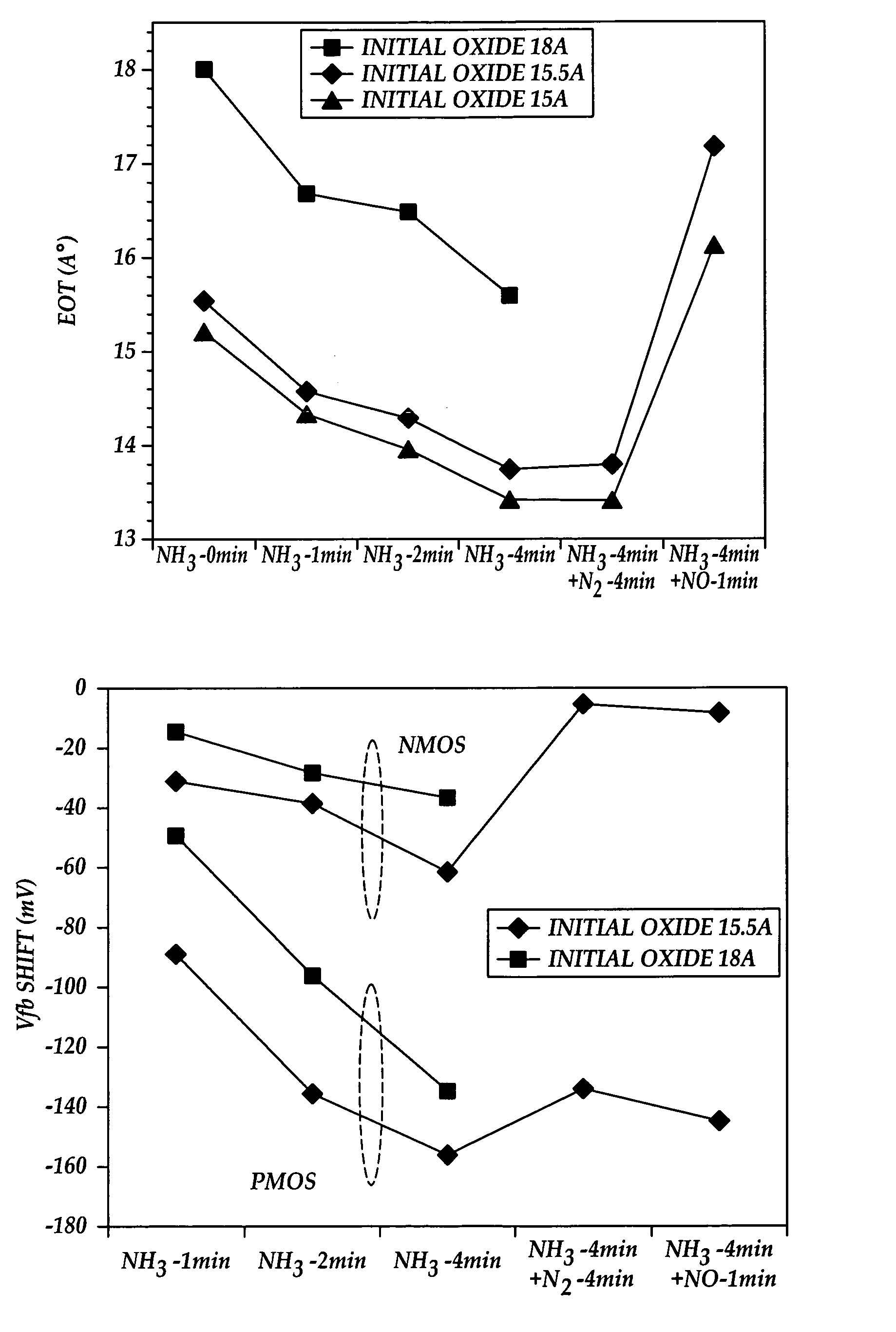
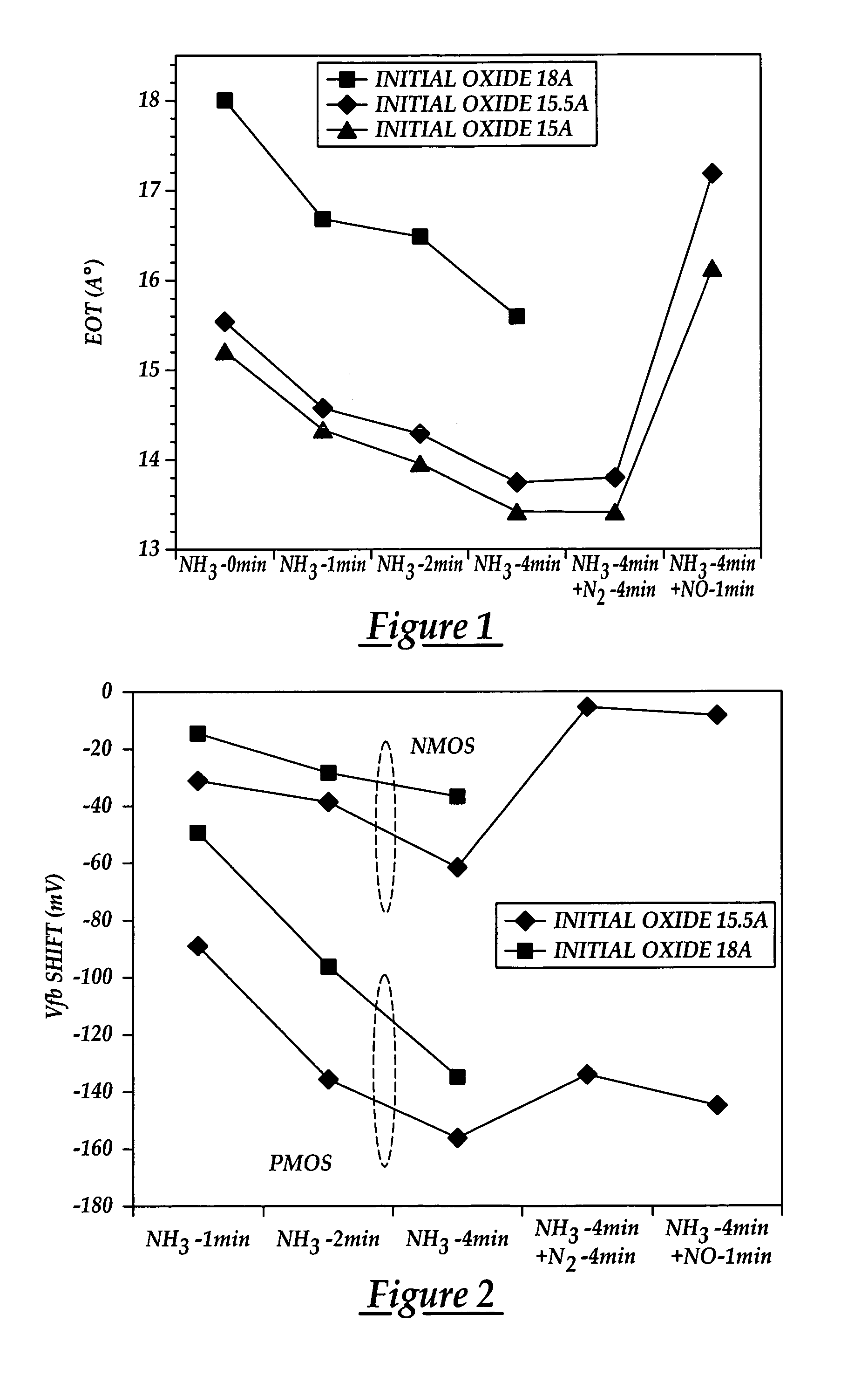
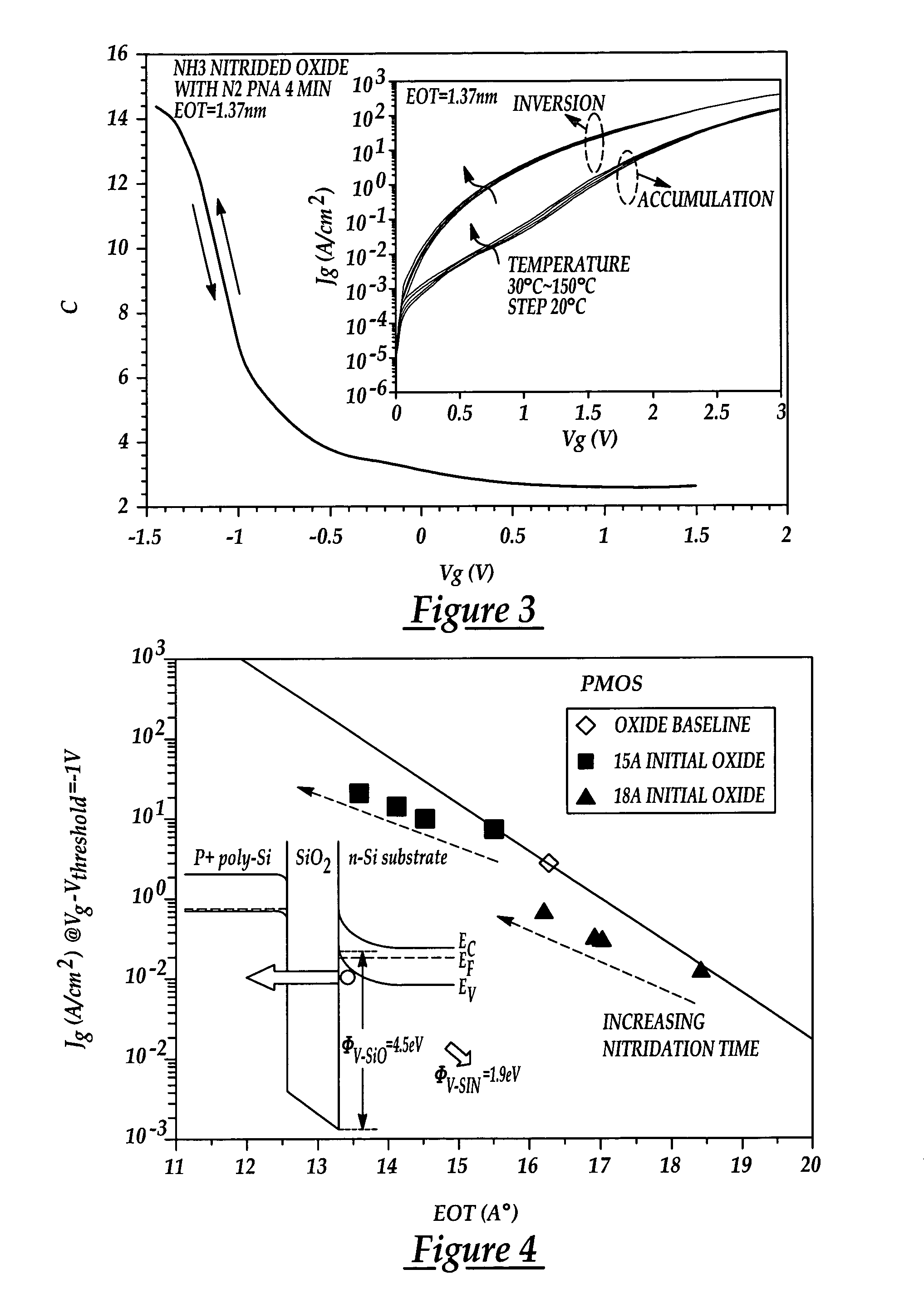
[0046]In this work, we profoundly investigate the feasibility and characteristics of ultrathin (EOT 13–16 Å) NH3 nitrided oxides. Oxide thickness was thick in the past time, and most of the studies of NH3 nitridation performed on these thick oxides were focused on the reliability improvement accompany with the nitrogen incorporation. No attention was paid on the EOT reduction through nitridation. For thick oxide (˜100 Å), 2–3 Å EOT reduction shows little influence on the characteristics. However, for oxide thickness down to the range of 10–20 Å in direct tunneling region, 2 Å EOT reduction can contribute to one order lower in gate leakage current. Opposite to the N2O nitridation and RPN which will cause an increase in film physical thickness, NH3 nitridation not only effectively introduce the nitrogen into gate oxide but also essentially keep unchanged in physical thickness. This property indicates the promising for NH3 nitridation in oxide equivalent thickness downscaling. The resu...


PUM


Abstract

A method of making a semiconductor device having a silicon dioxide based gate with improved dielectric properties including providing a silicon based substrate having active areas defined therein. Thermally growing a silicon dioxide based gate from the silicon based substrate. Nitriding the silicon dioxide based gate to provide a nitrided silicon dioxide based gate and to increase the dielectric constant of the silicon dioxide based gate without substantially increasing thickness of the silicon dioxide based gate.

Description

FIELD OF THE INVENTION[0001]This invention relates to a method of making an ultrathin silicon dioxide gate with improved dielectric properties by nitriding the silicon dioxide gate using NH3.BACKGROUND OF THE INVENTION[0002]The ultrathin gate dielectric has been emerged as one of the hardest challenges for further device scaling. Direct tunneling currents restrict the utilization of SiO2 films below approximately 1.5 nm thickness where tunneling currents larger than 1 A / cm2 are observed. Further reduction in thickness will increase tunneling current exponentially. Unacceptable gate leakage currents phase-out this gate dielectric material as early as the 0.1 μm CMOS process. The requirements summarized in the International Roadmap for Semiconductors (ITRS 1999) indicate the equivalent oxide thickness (EOT) progressing to substantially 1.0–1.5 nm for the 0.1 μm notes. No suitable alternative high dielectric constant material and interface layer has been identified with the stability a...

Claims


Application Information

Patent Timeline
IPC IPC(8): H01L21/336H01L21/8234H01L21/28H01L21/314H01L21/316H01L21/8238H01L29/51
CPCH01L21/28185H01L21/28202H01L29/518H01L21/823857H01L21/3144H01L21/31662H01L21/022H01L21/02238
Inventor WANG, MING-FANGCHEN, CHIEN-HAOYAO, LIANG-GICHEN, SHIH-CHANG
Owner TAIWAN SEMICON MFG CO LTD
Why Eureka
Try Eureka