Thin tungsten silicide layer deposition and gate metal integration

a technology of thin tungsten silicide and gate metal, which is applied in the direction of basic electric elements, electrical equipment, semiconductor devices, etc., can solve the problems of unsatisfactory interactions, affecting the resistance of the gate electrode and device reliability,

Inactive Publication Date: 2006-02-02
APPLIED MATERIALS INC +1
View PDF45 Cites 31 Cited by
  • Summary
  • Abstract
  • Description
  • Claims
  • Application Information

AI Technical Summary

Benefits of technology

[0012] In a further embodiment, a method of depositing layers of a gate electrode on a substrate comprising depositing a polysilicon layer on the substrate, depositing a layer having a thickness of between a

Problems solved by technology

However, it has been found that the treatment of such gate electrodes with subsequent processing steps, such as annealing, can result in undesirable interactions between the tungsten or tungst

Method used


Image

  • Thin tungsten silicide layer deposition and gate metal integration
  • Thin tungsten silicide layer deposition and gate metal integration
  • Thin tungsten silicide layer deposition and gate metal integration

Examples


example

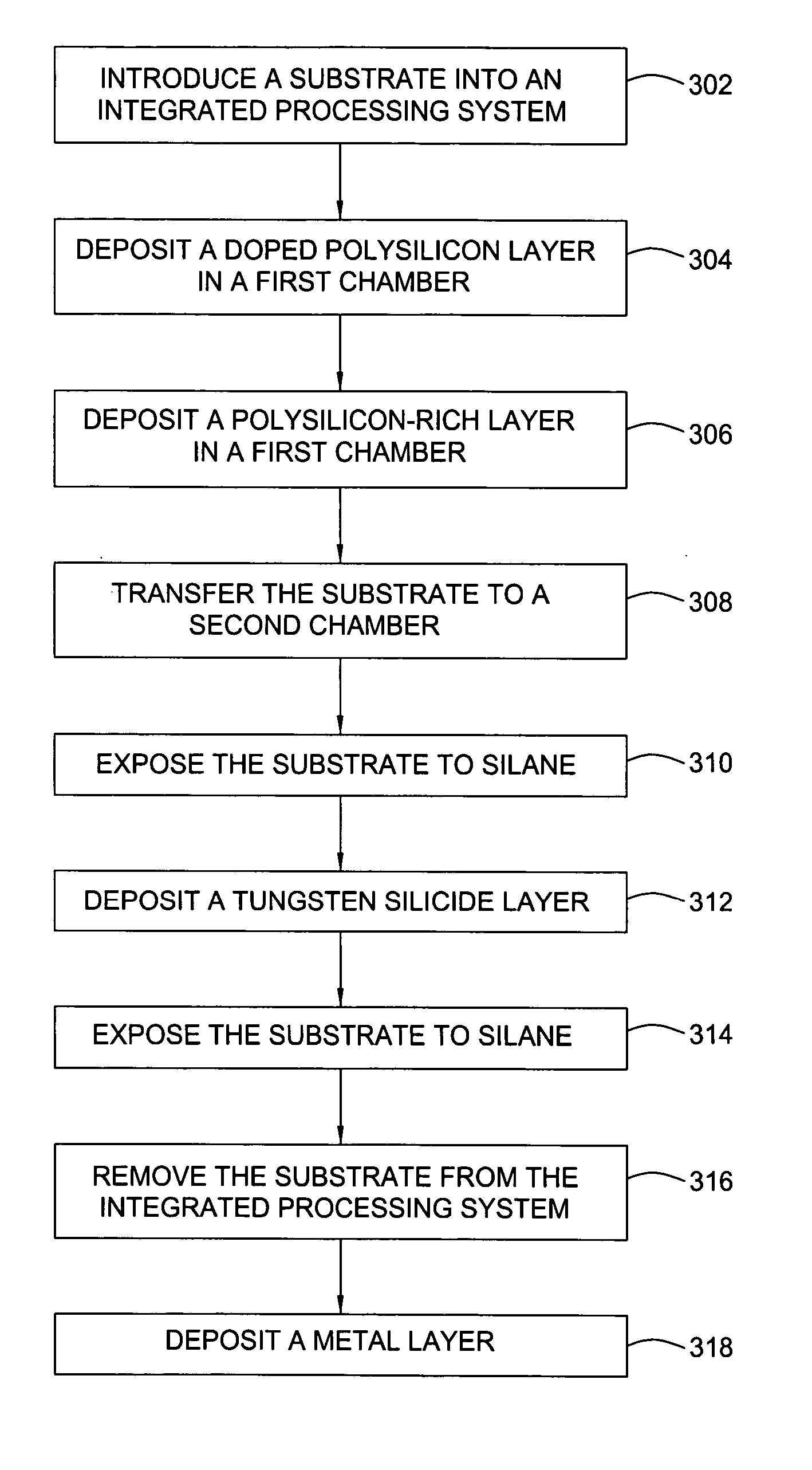
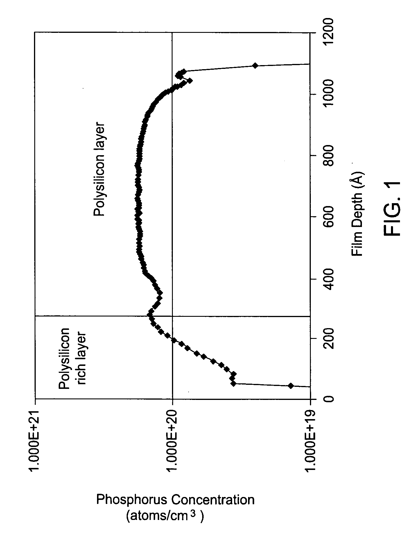
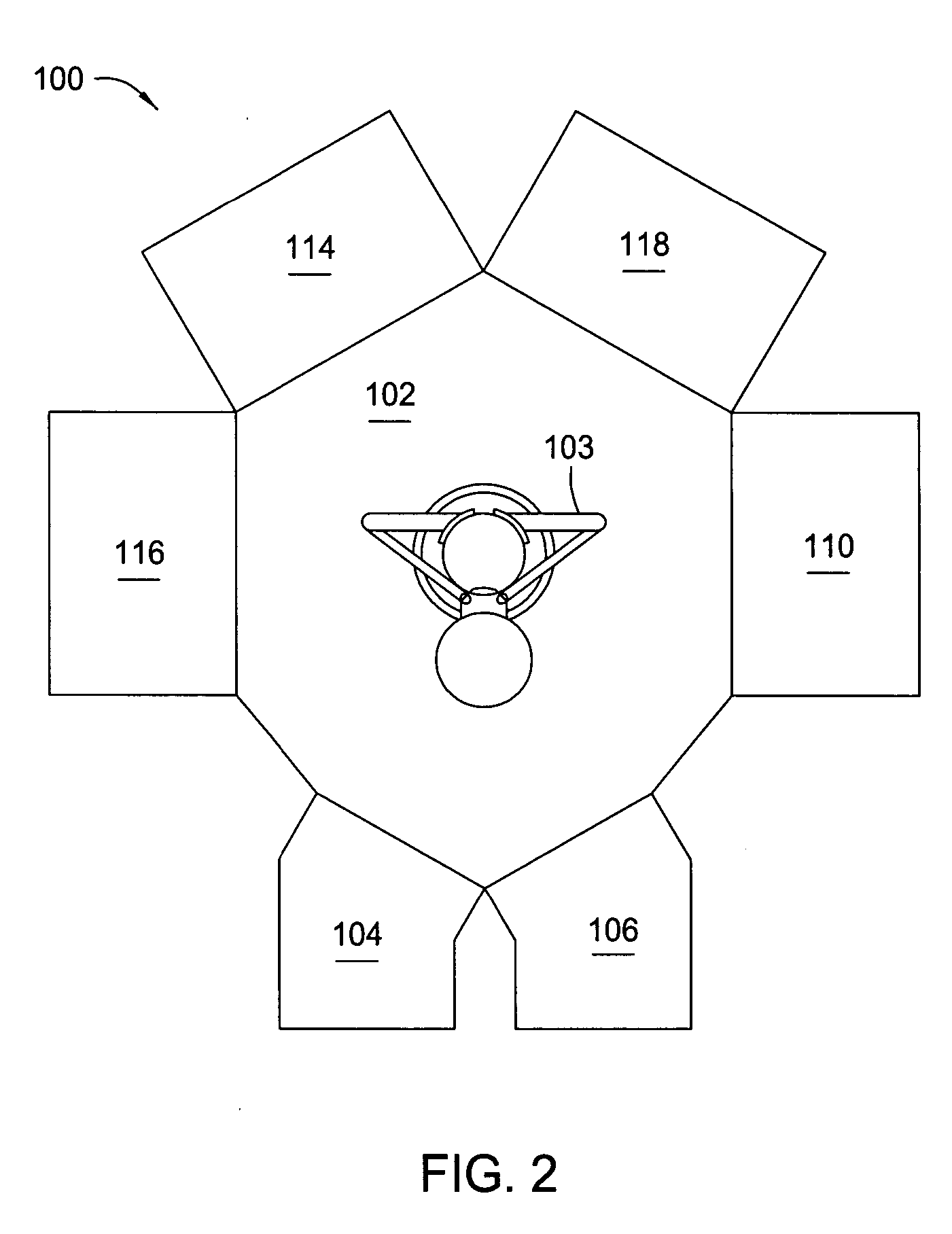
[0044] A 300 mm substrate having an oxide layer formed thereon was introduced into a Polycide Centura® system comprising a POLYgen™ chamber and a DCS xZ 300 chamber. A doped polysilicon layer was deposited on the substrate in a POLYgen™ chamber using a thermal chemical vapor deposition process from a gas mixture comprising silane and 1% phosphine diluted with hydrogen. The doped polysilicon layer was deposited at a pressure of 150 Torr with a phosphine flow rate of 99 sccm and a disilane flow rate of 50 sccm for about 55 seconds at a substrate support temperature of 600° C. and a substrate temperature of approximately 558° C. Nitrogen was flowed into the chamber prior to the deposition and was continued during and after the deposition. An undoped polysilicon layer was then deposited on the doped polysilicon layer using a disilane flow rate of 80 sccm for about 25 seconds, a pressure of 150 Torr, and a substrate support temperature of 600° C. and a substrate temperature of approximat...


PUM


Abstract

A method for depositing layers of a gate electrode is provided. The method includes depositing a doped polysilicon layer, a thin tungsten silicide layer, and a metal layer. In one aspect, the doped polysilicon layer and the thin tungsten silicide layer are deposited within an integrated processing system. In a further aspect, depositing the thin tungsten silicide layer includes exposing a polysilicon layer to a silicon source, depositing a tungsten silicide layer, and exposing the tungsten suicide layer to a silicon source.

Description

CROSS-REFERENCE TO RELATED APPLICATIONS [0001] This application claims benefit of U.S. Provisional Patent Application Ser. No. 60 / 592,585, filed Jul. 30, 2004, which is herein incorporated by reference.BACKGROUND OF THE INVENTION [0002] 1. Field of the Invention [0003] Embodiments of the present invention generally relate to methods of depositing layers of a gate electrode. [0004] 2. Description of the Related Art [0005] Integrated circuits are composed of many, e.g., millions, of devices such as transistors, capacitors, and resistors. Transistors, such as field effect transistors, typically include a source, a drain, and a gate stack. The gate stack typically includes a substrate, such as a silicon substrate, a gate dielectric, such as silicon dioxide (SiO2) on the substrate, and a gate electrode on the gate dielectric. [0006] Materials that have been used for gate electrodes include metals, such as aluminum (Al), and polysilicon. Doped polysilicon has become a preferred material f...

Claims


Application Information

Patent Timeline
IPC IPC(8): H01L21/8238H01L21/4763
CPCH01L21/28061H01L29/4941H01L29/4933H01L21/32053
Inventor LI, MINGWANG, SHULIN
Owner APPLIED MATERIALS INC
Why Eureka
Try Eureka