Method of fabricating single-layer and multi-layer single crystalline silicon and silicon devices on plastic using sacrificial glass

Inactive Publication Date: 2006-02-09
SHARP KK
View PDF13 Cites 87 Cited by
  • Summary
  • Abstract
  • Description
  • Claims
  • Application Information

AI Technical Summary

Benefits of technology

[0006] A method of fabricating a silicon-on-glass layer via layer transfer includes preparing a silicon substrate; depositing a layer of SiGe on the silicon substrate; depositing a layer of silicon on the SiGe layer; depositing a layer of insulator on the silicon layer; implanting splitting hydrogen ions into the silicon substrate; preparing a glass substrate; bonding the glass substrate to the silicon layer to form a composite wafer; splitting the composite wafer to provide a split wafer having, in seriatim, a glass substrate, a layer of silicon; a layer of SiGe; and silicon layer split from the silicon substrate; dry etching the split wafer to remove the silicon layer split from the silicon substrate and a portion of the SiGe layer; annealing the split wa

Problems solved by technology

Devices fabricated on plastic are light weight,

Method used


Image

  • Method of fabricating single-layer and multi-layer single crystalline silicon and silicon devices on plastic using sacrificial glass
  • Method of fabricating single-layer and multi-layer single crystalline silicon and silicon devices on plastic using sacrificial glass
  • Method of fabricating single-layer and multi-layer single crystalline silicon and silicon devices on plastic using sacrificial glass

Examples


Embodiment Construction

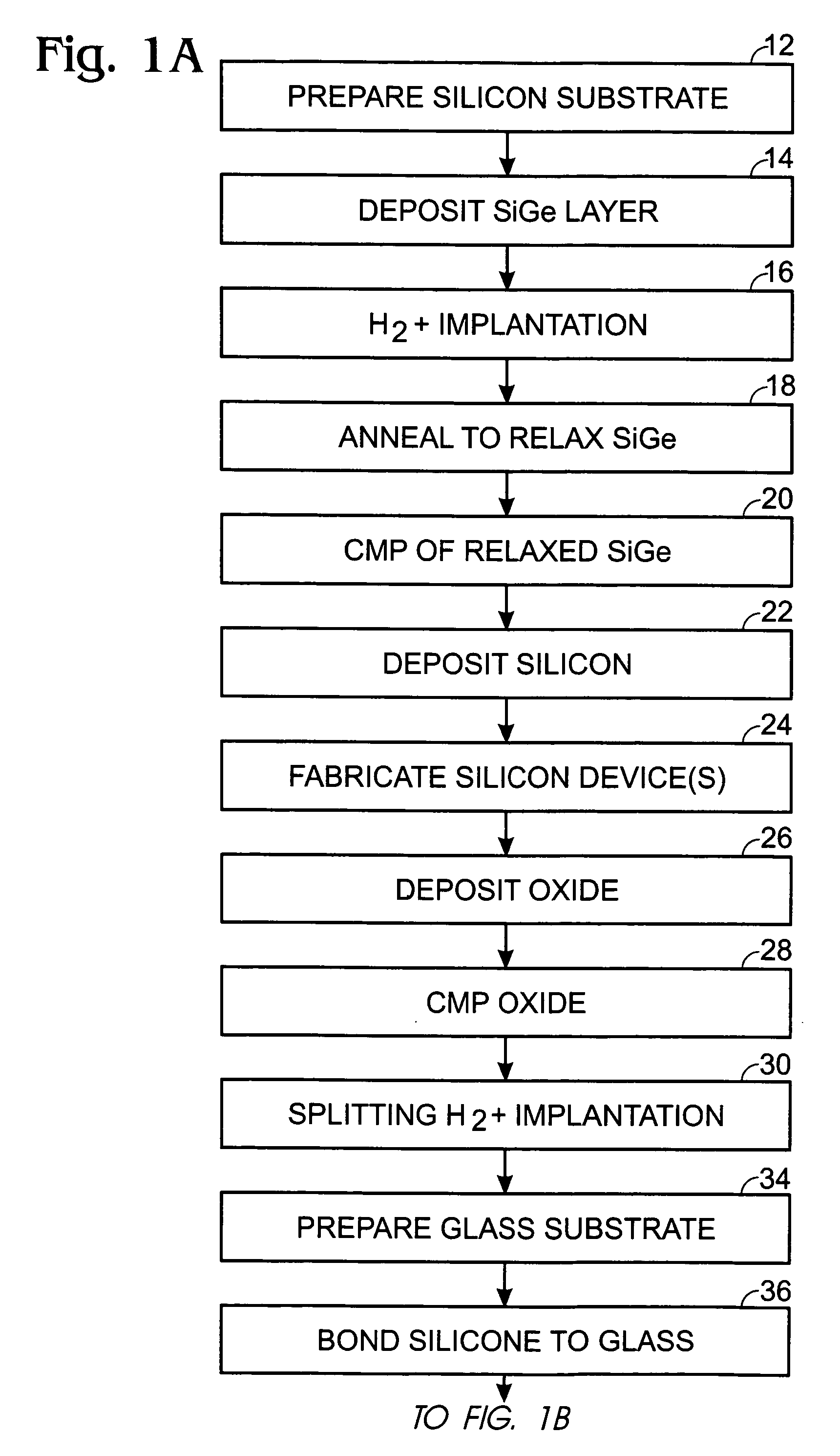
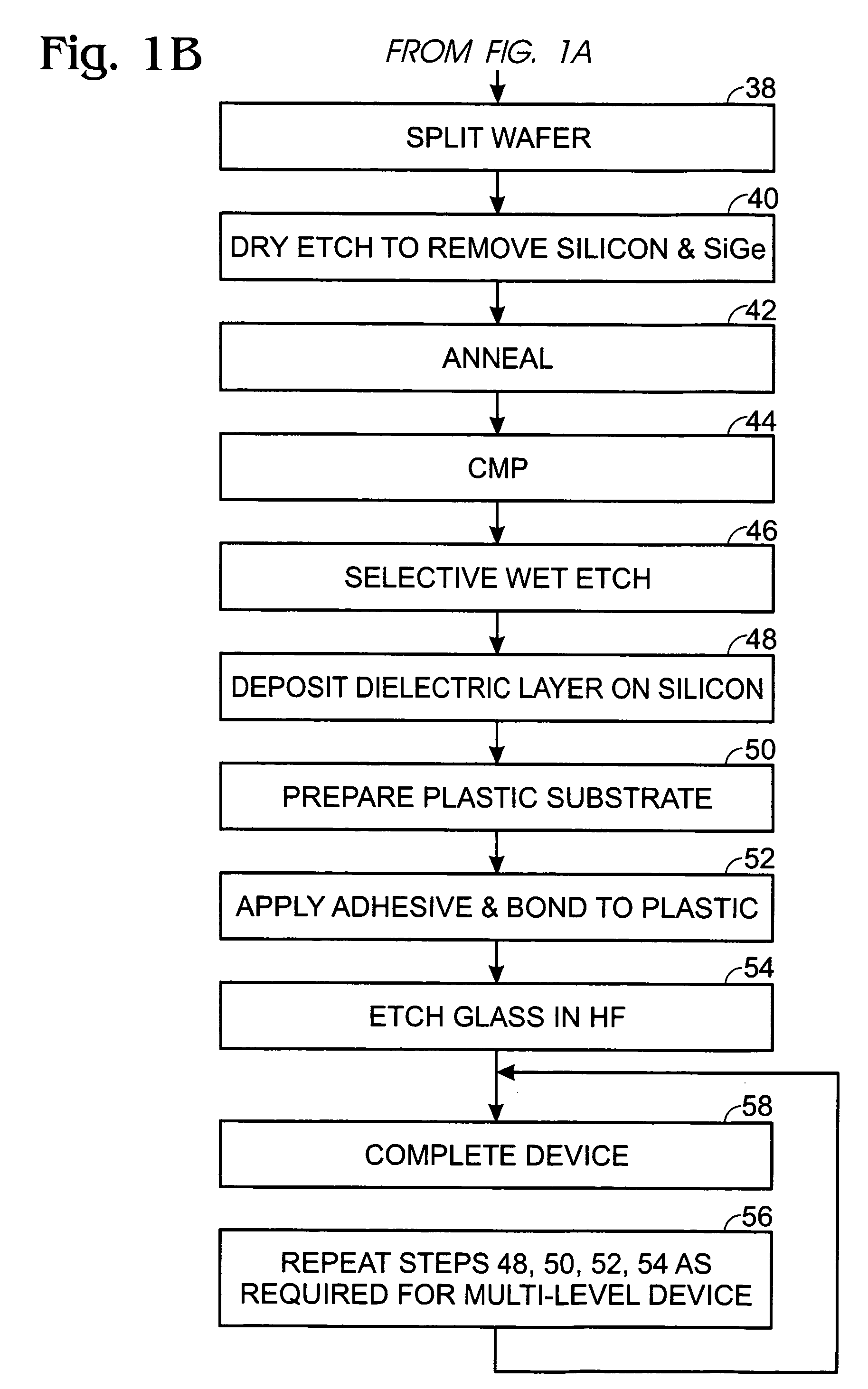
[0018] Unlike the above-identified prior art methods, a process is described herein to fabricate a high quality thin single crystalline silicon and silicon-based devices, and to then transfer the silicon, or silicon-based, device onto a plastic substrate.

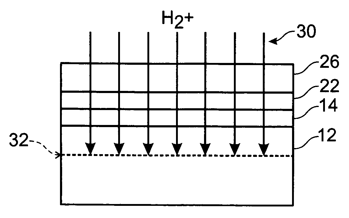
[0019] The method of the invention includes fabrication of a single crystalline silicon layer and silicon-based devices on plastic substrate. The silicon may be either strained or unstrained. A strained silicon layer is first formed on a relaxed SiGe layer by hydrogen-implantation-induced relaxation. The strained silicon film is transferred to a sacrificial glass substrate by direct wafer bonding and hydrogen induced exfoliation. The method of the invention is similar to that described in Ser. No. ______, filed ______ for Method of Fabricating Silicon-on-glass via Layer Transfer, which disclosure is incorporated herein by reference, however, the additional steps described herein result in a single, or multi, level silicon layer, or...


PUM


Abstract

A method of fabricating a silicon-on-plastic layer via layer transfer includes depositing a layer of SiGe on a silicon substrate; depositing a layer of silicon; implanting splitting hydrogen ions into the silicon substrate; bonding a glass substrate to the silicon layer; splitting the wafer; removing the silicon layer and a portion of the SiGe layer; depositing a dielectric on the silicon side of the silicon-on-glass wafer; applying adhesive and bonding a plastic substrate to the silicon side of the silicon-on-glass wafer; removing the glass from the glass side of the bonded, silicon-on-glass wafer to form a silicon-on-plastic wafer; and completing a desired IC device on the silicon-on-plastic. Multi-level structure may be fabricated according to the method of the invention by repeating the last few steps of the method of the invention.

Description

FIELD OF THE INVENTION [0001] This invention relates to fabrication of silicon-on-plastic, for display, sensor and mobile devices applications. BACKGROUND OF THE INVENTION [0002] The introduction of mobile devices, such as cellular phones, PDAs, electronic books, electronic newspapers, portable TV, etc., the use of thin film devices on plastic has dramatically increased. Devices fabricated on plastic are light weight, thinner than glass, and generally unbreakable. The most noticeable progress is the development of organic light emitting diode (OLED) display on plastic substrate was reported by Yoshida et al., 3-inch Full-color OLED Display using a Plastic Substrate, SID Digest, p. 856 (2003), however, the quality and resolution of the disclosed OLED display still requires further improvement to compete with silicon-based thin-film transistor (TFT) technology. [0003] Another approach is to fabricate TFTs directly on plastic substrate, as described by Okada et al., A 4-in Reflective C...

Claims


Application Information

Patent Timeline
IPC IPC(8): H01L21/30H01L21/20
CPCH01L21/187H01L21/26506Y10S438/977H01L2221/6835H01L2221/68368H01L21/6835
Inventor MAA, JER-SHENLEE, JONG-JANTWEET, DOUGLAS J.HSU, SHENG TENG
Owner SHARP KK
Why Eureka
Try Eureka