[0071] In case where much light directly goes outside from the light-emitting element without passing through the wavelength-conversion portion, the quantity of light capable of being converted to have a desired wavelength is reduced and the radiative
light intensity is also reduced. However, where the light-reflecting portion is so positioned that its outer periphery is on the side of the second reflecting portion with respect to the line that runs prom the edge of the light-emitting element to the upper edge of the inner
peripheral surface of the first reflecting portion opposite to the edge of the light-emitting element, the quantity of light from the light-emitting element that is directly radiated outside the apparatus through a gap between the light-reflecting portion and the first reflecting portion can be reduced. In that manner, a major part of the light from the light-emitting element can be led through the wavelength-conversion portion, and therefore the quantity of light that undergoes
wavelength conversion can be increased whereby the
wavelength conversion efficiency is improved and the light having a desired wavelength spectrum can be radiated from the apparatus with
high intensity.
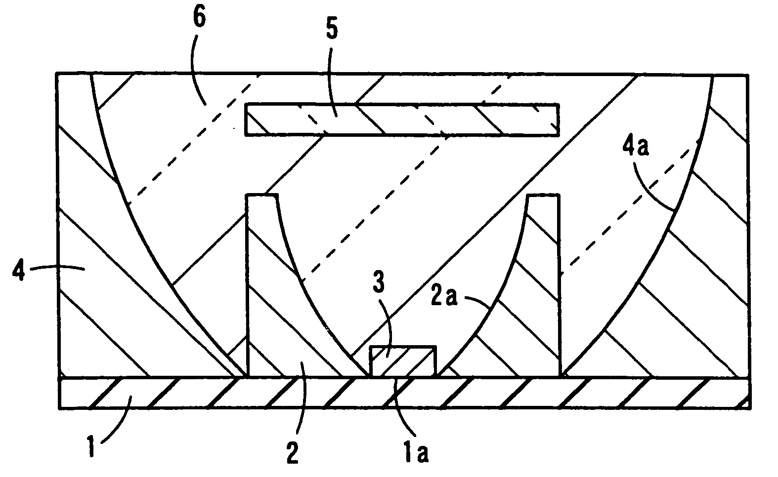
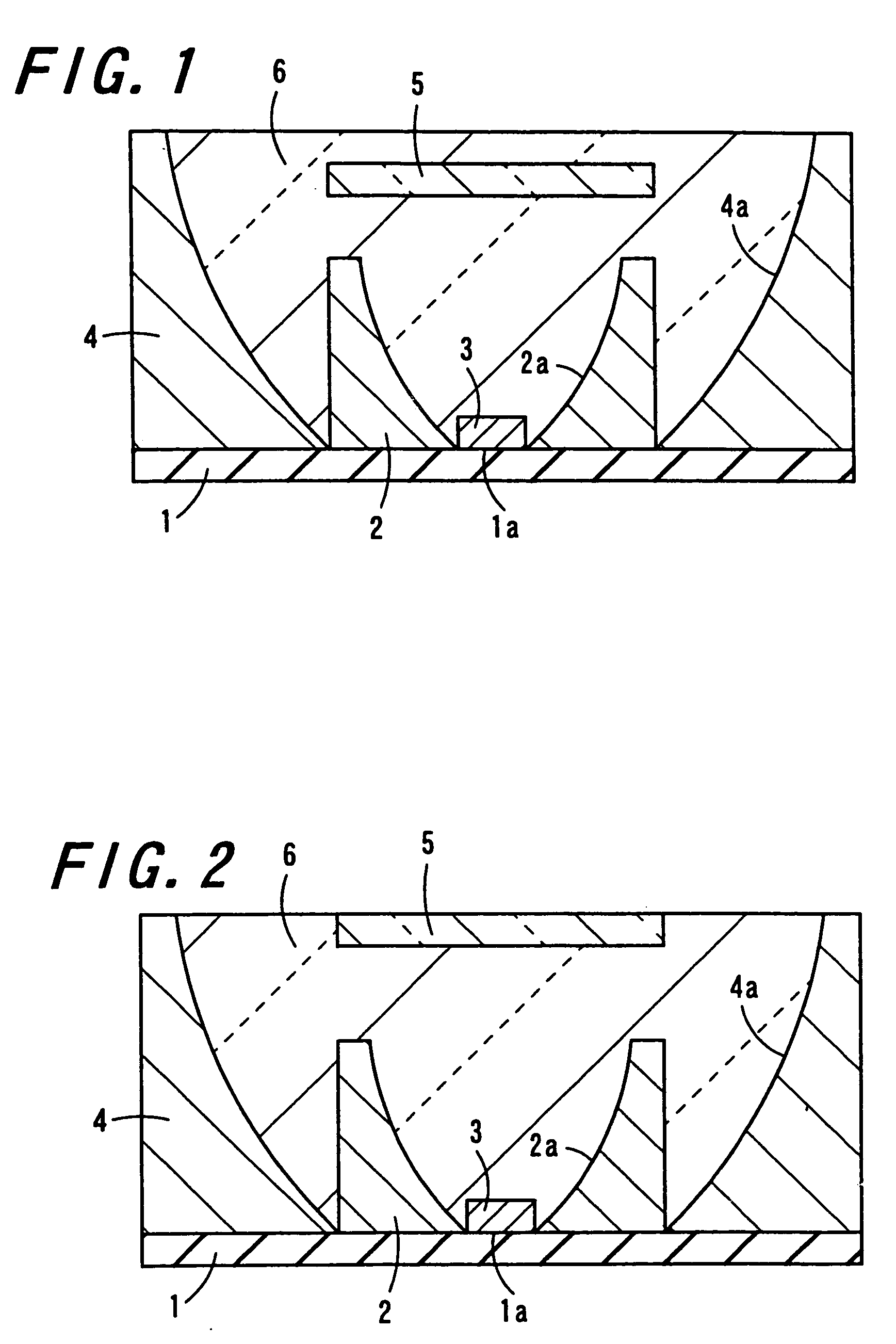
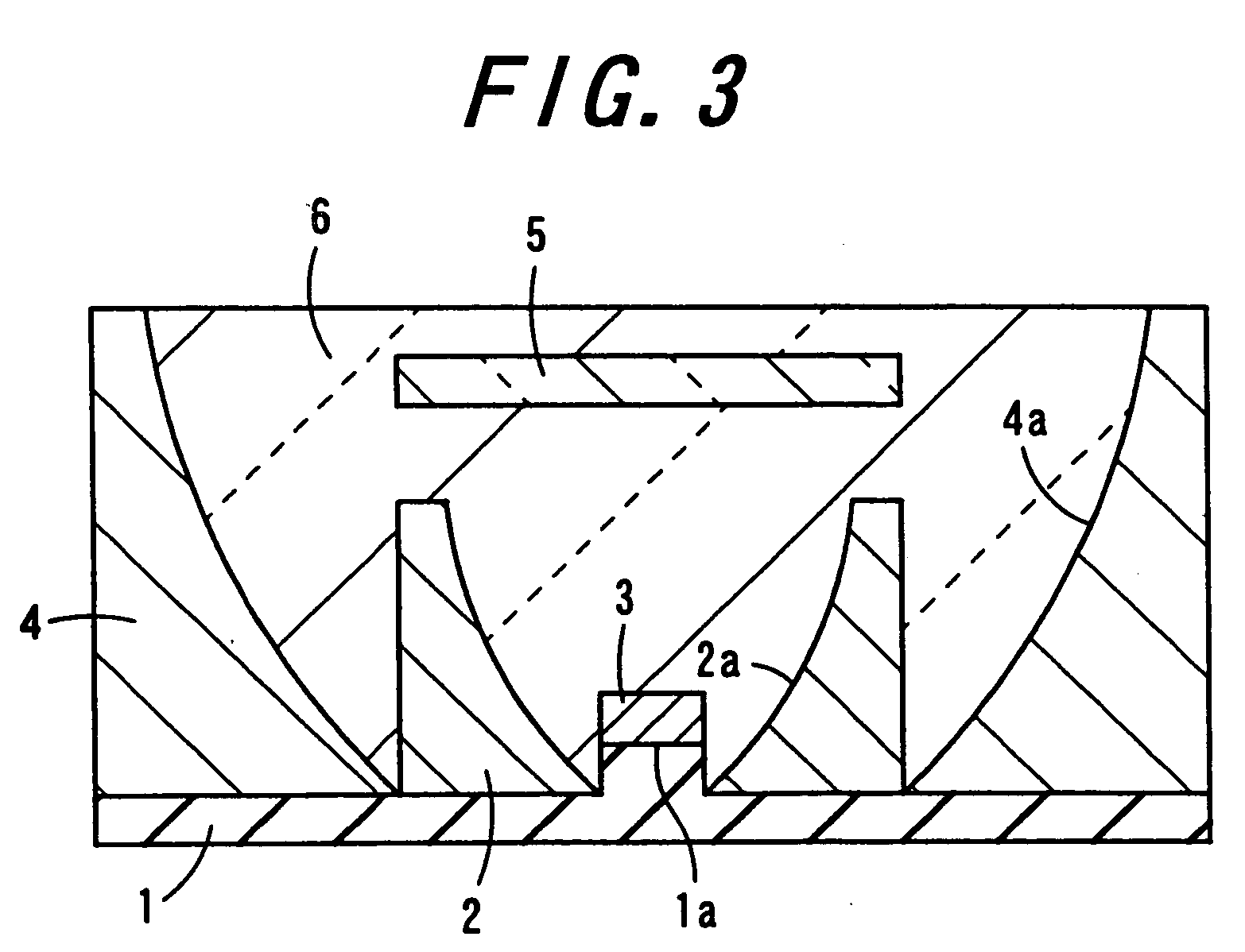
[0072] According to the invention, since the light-reflecting portion has a light-scattering surface facing the light-emitting element, it is possible to effectively reflect the light from the light-emitting element downward and outward, so that the reflected light can be led inside the wavelength-conversion portion.
[0061] According to the invention, in the light-emitting apparatus, the second reflecting portion has, on its inner
peripheral surface, a second wavelength-conversion portion for converting the wavelength of the light from the light-emitting element. Accordingly, the light from the light-emitting element that has been reflected downward without
wavelength conversion in the first wavelength-conversion portion can undergo wavelength conversion in the second wavelength-conversion portion, and therefore, it is possible to improve radiative
light intensity, brightness and luminous efficiency.
[0073] According to the invention, the second wavelength-conversion portion or the wavelength-conversion portion is so formed that its thickness gradually increases from its upper end to its lower end. Accordingly, the quantity of light from the
phosphor material gradually increases toward the lower end of the second wavelength-conversion portion or the wavelength-conversion portion at which the distance between the upper surface of the light transmitting member and the second wavelength-conversion portion or the wavelength-conversion portion is larger, but toward the upper end of the second wavelength-conversion portion or the wavelength-conversion portion at which the distance between the upper surface of the light transmitting member and the second wavelength-conversion portion or the wavelength-conversion portion is smaller, the quantity of light from the
phosphor material is gradually smaller than that toward the lower end thereof. As a result, the light intensity distribution in the light-emitting apparatus can be made uniform in the center part and in the
peripheral part of the apparatus, and color unevenness is prevented from occurring in the apparatus.
[0075] Further, the light from the light-emitting element that has been reflected downward and outward without wavelength conversion in the first wavelength-conversion portion can undergo wavelength conversion by the action of the
phosphor material having an increased density, and therefore, in the light-emitting apparatus, high radiative light intensity, high brightness and improved luminous efficiency are achieved.
[0076] According to the invention, the second wavelength-conversion portion or the wavelength-conversion portion is so formed that its inner surface has plural recesses or protrusions. Accordingly, the light from the light-emitting element that has been transmitted to the first wavelength-conversion portion directly or after reflection on the inner peripheral surface of the first reflecting portion, and has been reflected downward and outward and enters the second wavelength-conversion portion with no wavelength conversion by the action of the phosphor material contained in the first wavelength-conversion portion, or the light from the light-emitting element that has been transmitted to the light-reflecting portion directly or after reflection on the inner peripheral surface of the first reflecting portion, and has been reflected by the light-reflecting portion downward and outward and enters the wavelength-conversion portion, is readily led inside the second wavelength-conversion portion or the wavelength-conversion portion owing to the recesses and the protrusions, and, as a result, the light to undergo wavelength conversion by the action of the phosphor material in the second wavelength-conversion portion or the wavelength-conversion portion increases. Accordingly, in the light-emitting apparatus, high radiative light intensity, high brightness and improved luminous efficiency are archieved.
[0061] According to the invention, in the light-emitting apparatus, the second reflecting portion has, on its inner peripheral surface, a second wavelength-conversion portion for converting the wavelength of the light from the light-emitting element. Accordingly, the light from the light-emitting element that has been reflected downward without wavelength conversion in the first wavelength-conversion portion can undergo wavelength conversion in the second wavelength-conversion portion, and therefore, it is possible to improve radiative light intensity, brightness and luminous efficiency.
[0078] According to the invention, the height of the placement portion protrudes higher than the lower edge of the inner peripheral surface of the first reflecting portion. Accordingly, the light emitted by the light-emitting element in the oblique downward direction can be efficiently reflected upward on the inner peripheral surface of the first reflecting portion, and, as a result, the light from the light-emitting element can be prevented from being confined within the light-emitting apparatus by the lower edges of the inner peripheral surface of the first reflecting portion. Accordingly in the light-emitting apparatus of the type, the light
absorption loss on the inner peripheral surface of the first reflecting portion with respect to the light from the light-emitting element may be reduced. As a result, the radiative light intensity of the light-emitting apparatus can be increased.
[0079] According to the invention, the illuminating apparatus is constructed by setting up the light-emitting apparatus mentioned above in a predetermined arrangement. In this illuminating apparatus,
light emission is affected by exploiting recombination of electrons in the light-emitting element composed of a
semiconductor. Thus, the illuminating apparatus can be made compact and have the
advantage, in terms of
power saving and long lifetime, over a conventional illuminating apparatus for effecting
light emission through electrical
discharge. As a result, variation in the center wavelength of the light emitted from the light-emitting element can be suppressed; wherefore the illuminating apparatus is capable of irradiating light with stable
radiation light intensity and stable
radiation light angle (
luminous intensity distribution) for a longer period of time. Moreover, unevenness in color and unbalanced illumination distribution can be prevented from occurring on a to-be-irradiated surface.
[0080] Moreover, by setting up the light-emitting apparatuses of the invention in a predetermined arrangement as light sources, followed by arranging around the light emitting apparatuses such a component as is optically designed in a suitable configuration, for example a reflection jig, an optical lens, and a light
diffusion plate, it is possible to realize an illuminating apparatus which is capable of emitting light with suitable
luminous intensity distribution.

