

Spin cleaning and drying apparatus and method of spin cleaning and drying
a technology of spin cleaning and drying apparatus and spin cleaning and drying method, which is applied in the direction of cleaning process and apparatus, cleaning using liquids, chemistry apparatus and processes, etc., can solve the problems of insufficient drying of the peripheral part of the back surface of the wafer, and insufficient drying of the peripheral part of the wafer, etc., to achieve sufficient drying of the substrate
- Summary
- Abstract
- Description
- Claims
- Application Information
AI Technical Summary
Benefits of technology
Problems solved by technology
Method used
Image

Examples
Embodiment Construction
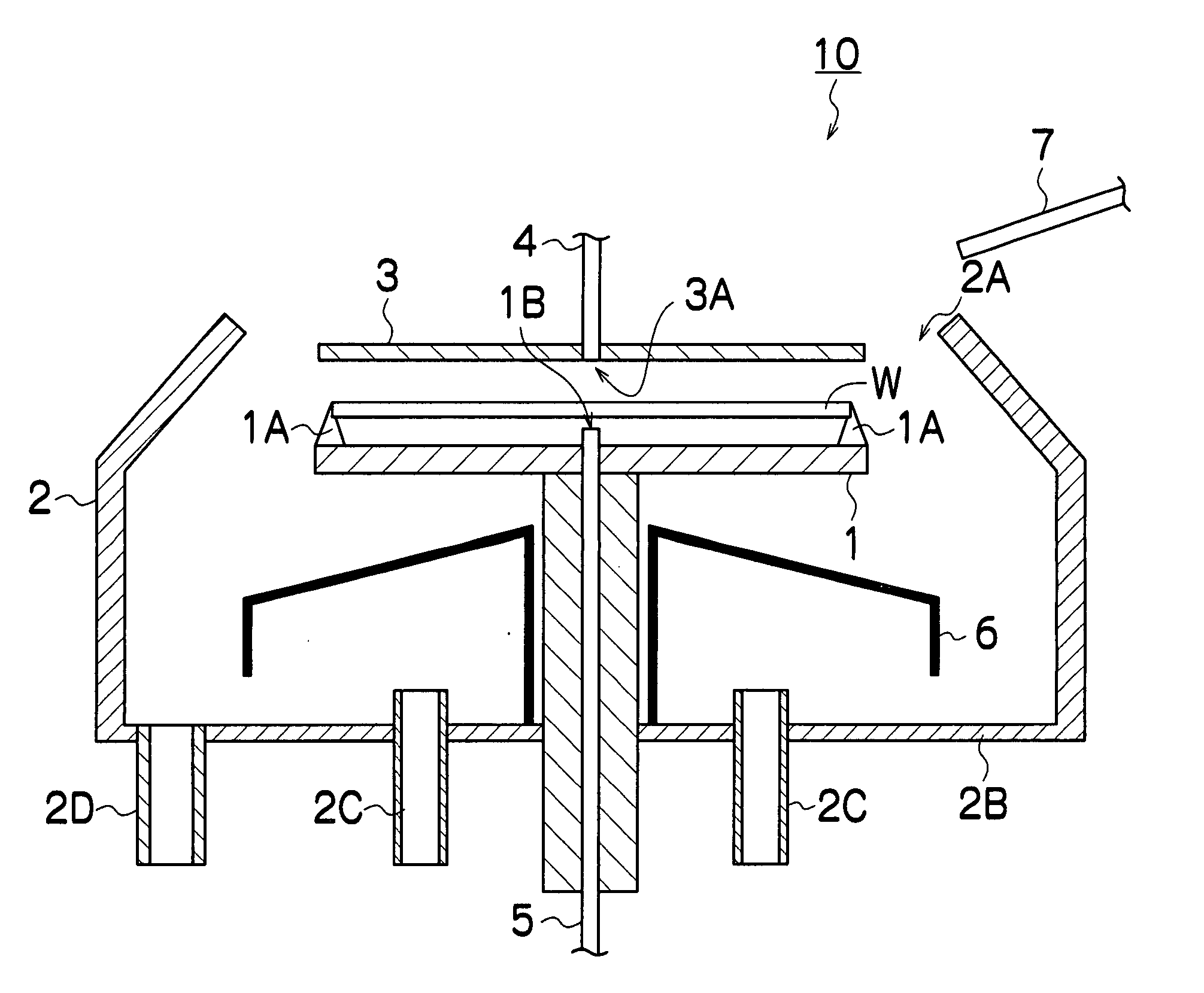
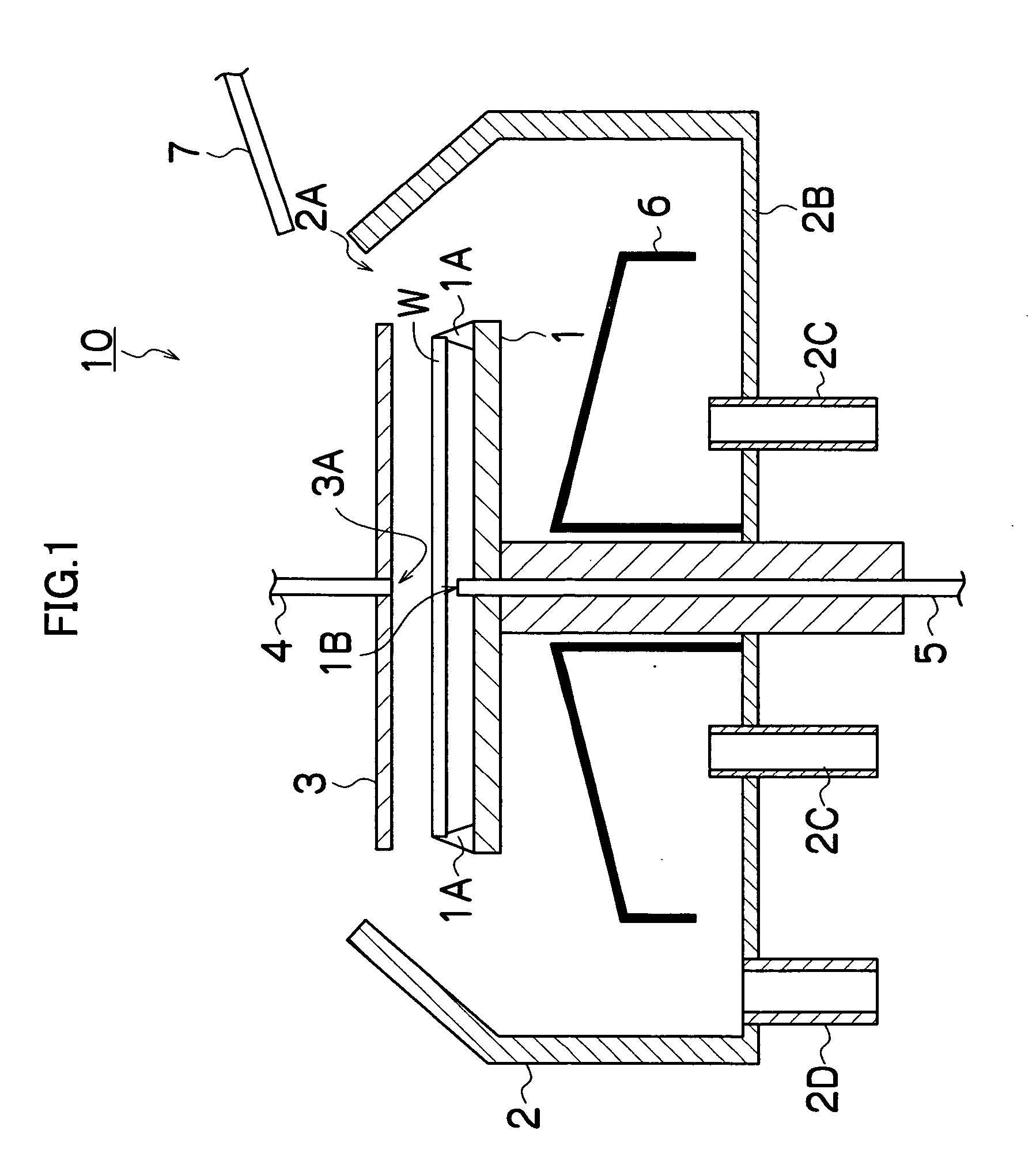
[0040] Preferred embodiments of a spin cleaning and drying apparatus and a spin cleaning and drying method according to the present invention will be described below on the basis of the accompanying drawings. Incidentally, like reference numerals or characters refer to like members in each of the drawings.
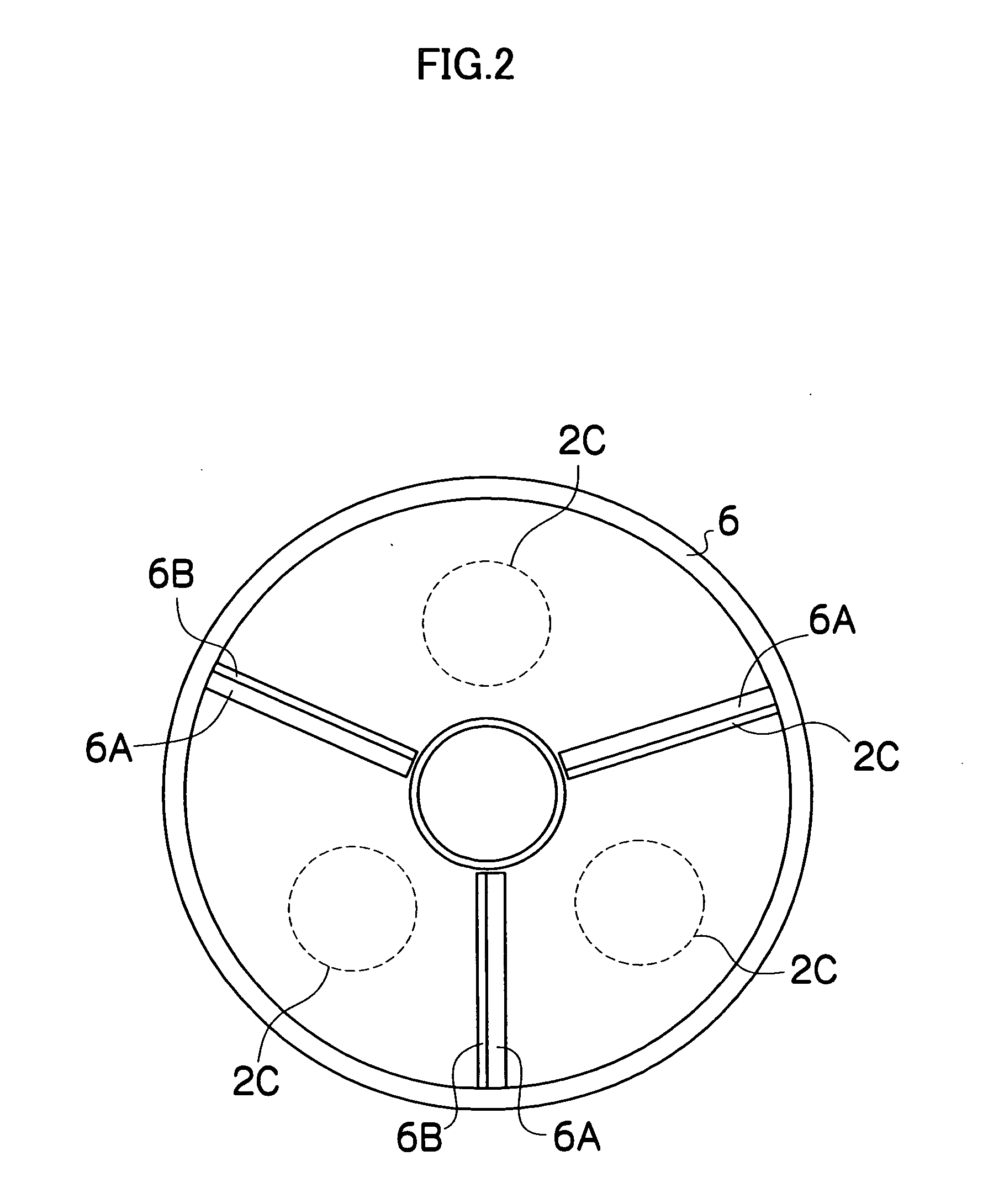
[0041]FIG. 1 is a sectional view of a spin cleaning and drying apparatus related to an embodiment of the present invention. The spin cleaning and drying apparatus 10 is constituted by a spin chuck 1 which has three supporting pins 1A, 1A, 1A, which support a wafer W on an upper surface, and spins, a cup 2 in an upper part of which an opening 2A is formed and which encloses the spin chuck 1, a flow regulating plate 3 which can move to a position opposed to the wafer W and spaced therefrom at a prescribed distance and to a position which is retracted upward, a rinse nozzle 7 which supplies a rinse liquid from the opening 2A of the cup 2 to the wafer W, an exhaust cover 6 which is pr...
PUM
| Property | Measurement | Unit |
|---|---|---|
| diameter | aaaaa | aaaaa |
| distance | aaaaa | aaaaa |
| electrically conductive | aaaaa | aaaaa |
Abstract
Description
Claims
Application Information