Vertical transistors

a technology of vertical transistors and transistors, applied in the field of integrated circuit fabrication, can solve the problems of difficult integration into the process flow of a dram memory cell, design can take up more chip real estate,

Active Publication Date: 2006-03-02
MICRON TECH INC
View PDF75 Cites 65 Cited by
  • Summary
  • Abstract
  • Description
  • Claims
  • Application Information

AI Technical Summary

Problems solved by technology

However, these designs can take up more chip real estate.
However, this c

Method used


Image

  • Vertical transistors
  • Vertical transistors
  • Vertical transistors

Examples


Embodiment Construction

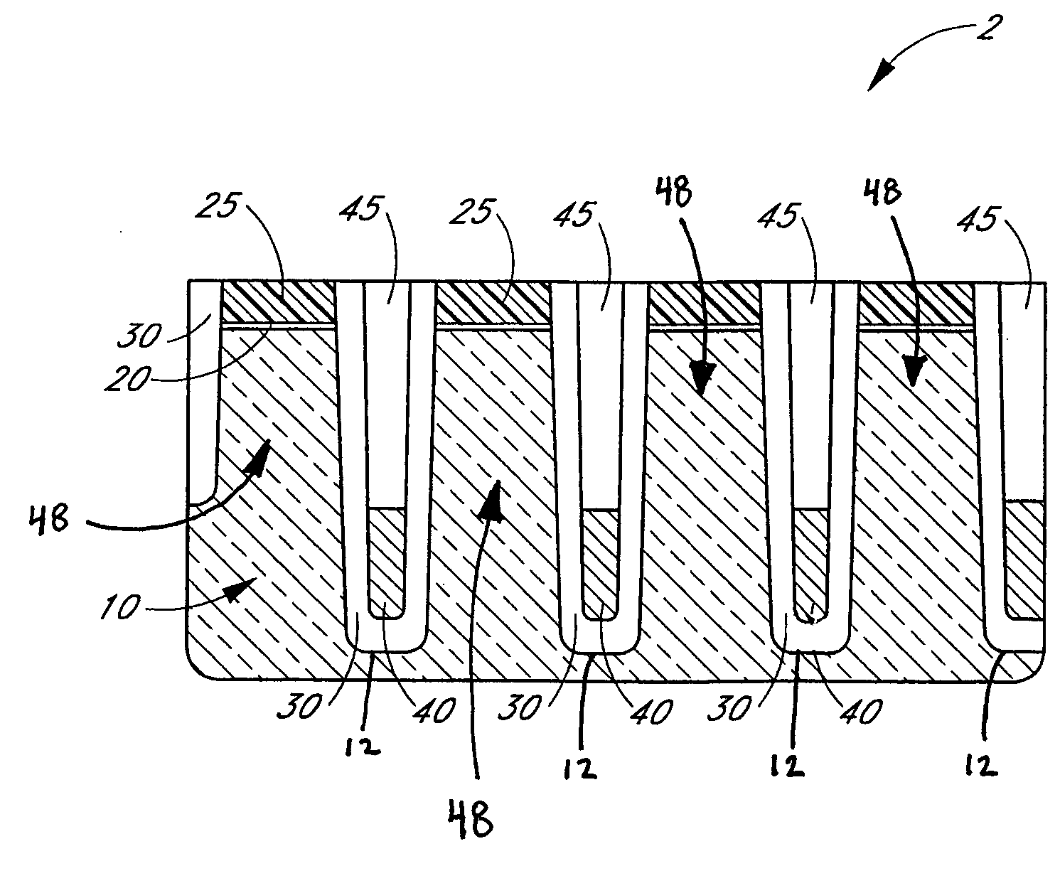
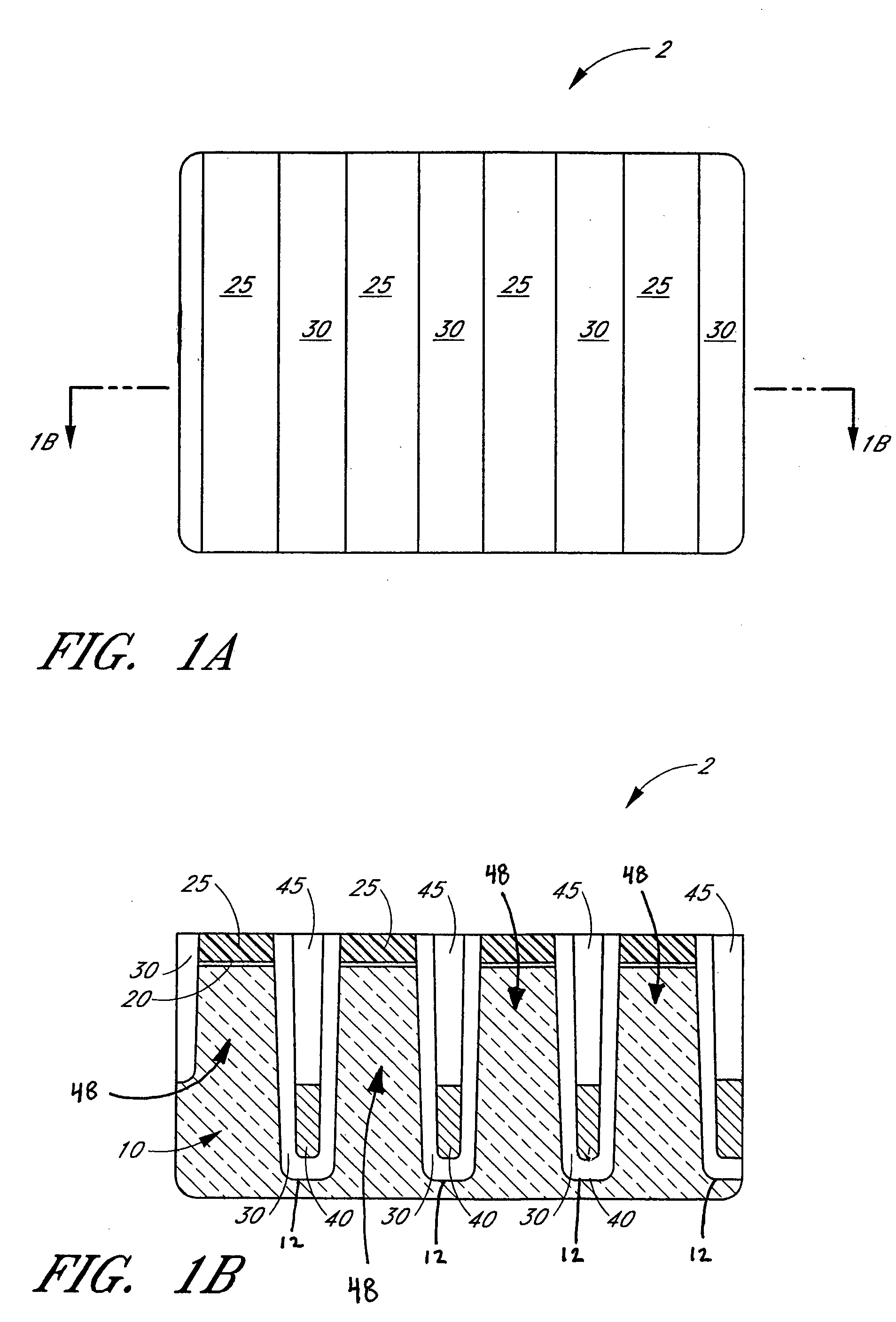
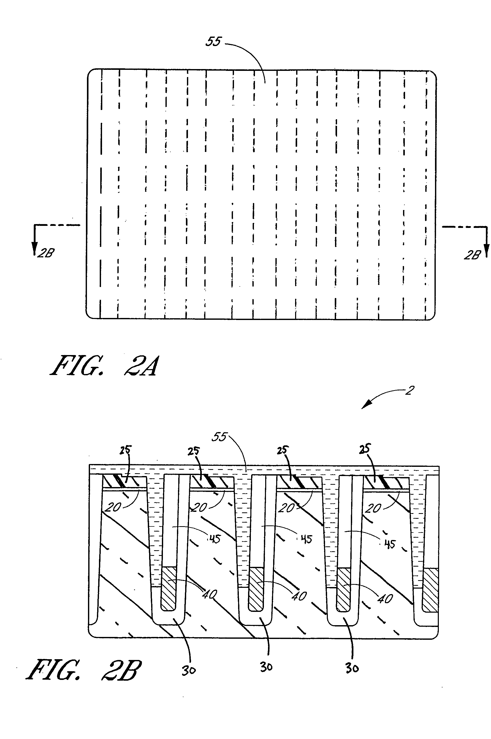
[0046] In the context of this document, the term “semiconductor substrate” is defined to mean any construction comprising semiconductor materials, including, but not limited to, bulk semiconductor materials such as a semiconductor wafers, and semiconductor material layers. The term “substrate” refers to any supporting substrate, including, but not limited to, the semiconductor substrates (either alone or in assemblies comprising other materials thereon) described above. Also in the context of this document, the term “layer” encompasses both the singular and the plural unless otherwise indicated.

[0047] Processes for forming vertical surround gate transistors (VSGTs), memory cells comprising VSGTs and arrays of same are disclosed. Preferably, the memory cells have a cell size of 4F2. In preferred embodiments, transistors are formed without using a separate interconnect outside of the isolation trench to connect a buried digit line and a lower active area. A digit line link within the...


PUM


Abstract

Vertical transistors for memory cells, such as 4F2 memory cells, are disclosed. The memory cells use digit line connections formed within the isolation trench to connect the digit line with the lower active area. Vertical transistor pillars can be formed from epitaxial silicon or etched from bulk silicon. Memory cells can be formed by creating a cell capacitor electrically connected to each transistor pillar.

Description

BACKGROUND OF THE INVENTION [0001] 1. Field of the Invention [0002] The present invention relates to the field of integrated circuit fabrication, specifically to the formation of transistors. [0003] 2. Description of the Related Art [0004] Since the introduction of the digital computer, electronic storage devices have been a vital resource for the retention of data. Conventional semiconductor electronic storage devices, such as Dynamic Random Access Memory (DRAM), typically incorporate capacitor and transistor structures in which the capacitors temporarily store data based on the charged state of the capacitor structure. In general, this type of semiconductor Random Access Memory (RAM) often requires densely packed capacitor structures that are easily accessible for electrical interconnection. [0005] In order to increase efficiency of memory devices, there is an effort to create smaller memory cells. DRAM memory cells can shrink in several ways. One way to decrease the size of a mem...

Claims


Application Information

Patent Timeline
IPC IPC(8): H01L29/94
CPCH01L21/28132H01L27/10814H01L29/66666H01L27/10885H01L27/10888H01L27/10876H10B12/315H10B12/053H10B12/482H10B12/485
Inventor TANG, SANH DANGHALLER, GORDON A.
Owner MICRON TECH INC
Why Eureka
Try Eureka