Electronic component package

Inactive Publication Date: 2006-03-02
MITSUBISHI ELECTRIC CORP
View PDF4 Cites 21 Cited by
  • Summary
  • Abstract
  • Description
  • Claims
  • Application Information

AI Technical Summary

Benefits of technology

[0012] The present invention has been made with a view toward solving the problems described above, and it is an object of the invention to provide an electronic component package that allows a solder fillet to be easily formed at an end surface of a lead so as to

Problems solved by technology

This material is used also for the leads 3 around the packages; however, using it as it is would not be compatible with solder because of an oxide film formed on its surface, which Is inconvenient for the leads 3.
As a result, no solder fillets are formed onto the end surface 3B, posing a problem in that it is difficult to check whether soldering to the circuit board 8 has been successfully accomplished when observed from above the package 6.
There has been another problem in that the leads 3 are strongly pressed downward from above by

Method used


Image

  • Electronic component package
  • Electronic component package
  • Electronic component package

Examples


first embodiment

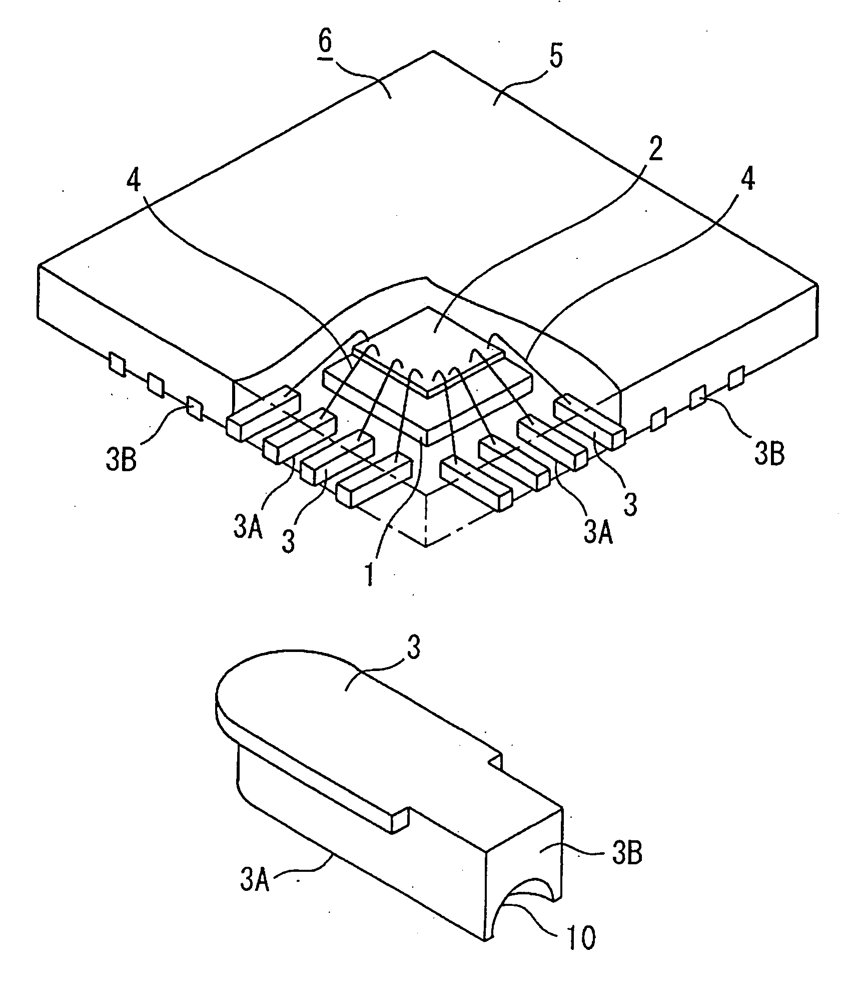
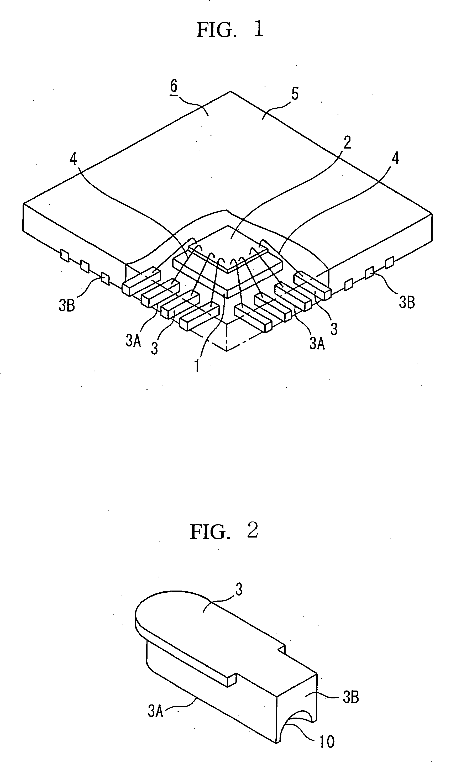
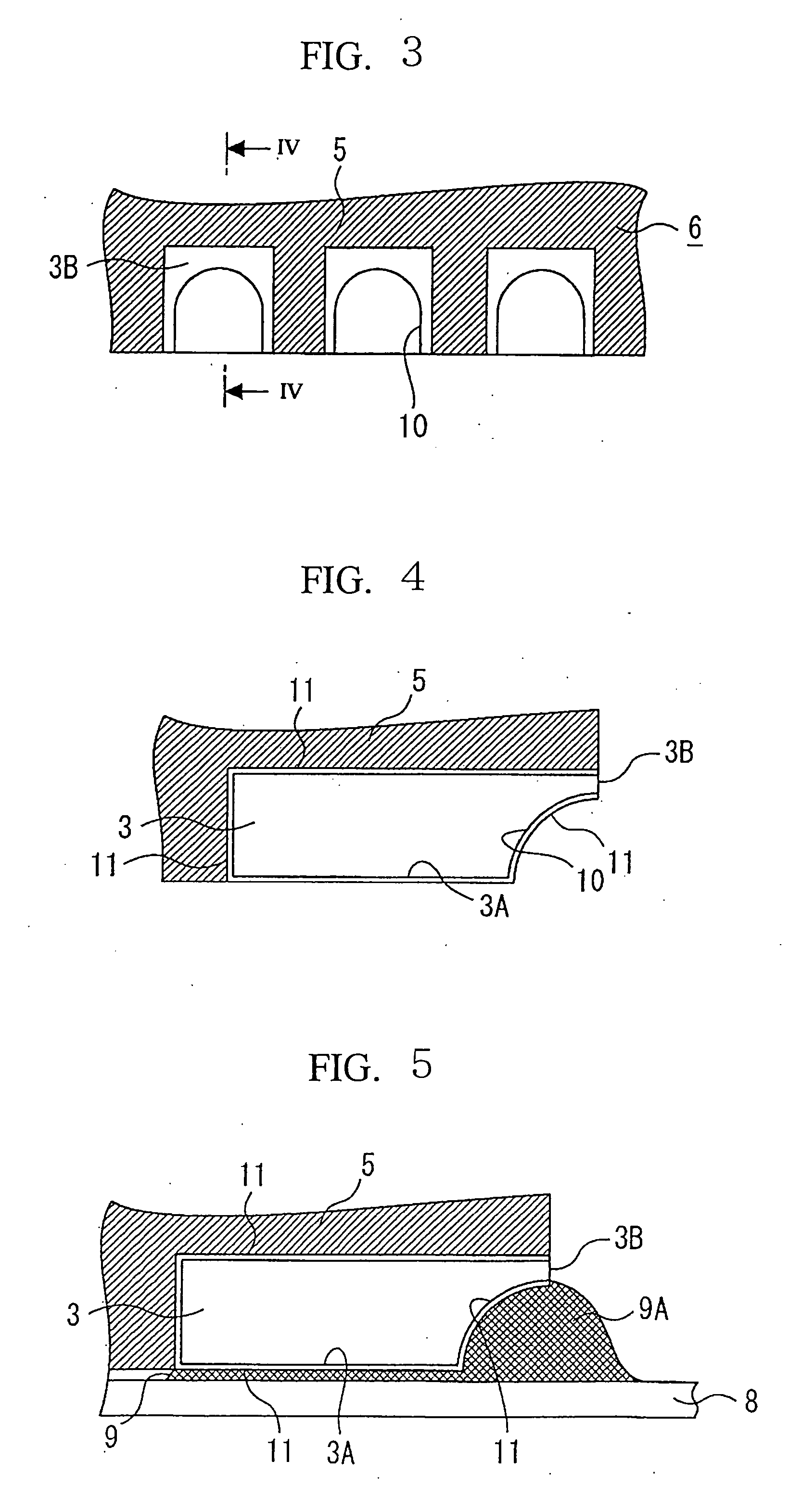
[0033] A first embodiment of the present invention will be described with reference to the accompanying drawings. FIG. 1 is a partly cutaway perspective view showing a schematic construction of the first embodiment. FIG. 2 is an enlarged view showing a construction of a lead of the first embodiment. FIG. 3 is a schematic diagram of a package observed from an external end surface side of leads.

[0034] As shown in the figures, a package 6 is constructed of an electronic component substrate 2, such as a semiconductor chip, disposed and secured on a dice pad 1, a plurality of leads 3 that are formed of a frame core material and arranged side by side around the dice pad 1, as in the prior art described above, wires 4 connecting signal pads of the semiconductor chip 2 and predetermined leads 3, and a molding resin 5 that seals the dice pad 1, the semiconductor chip 2, and the wires 4 such that bottom surfaces 3A and one end surfaces 3B of the leads 3 are exposed.

[0035] As shown in FIG. 2...

second embodiment

[0037] A second embodiment according to the present invention will now be explained in conjunction with the accompanying drawings. The construction of a package 6 is identical to that shown in FIG. 1 except for leads; therefore, the description will be omitted with the aid of FIG. 1.

[0038]FIG. 6 is an enlarged view showing the construction of a lead of the second embodiment. FIG. 7 is a schematic diagram showing the package 6 observed from an external end surface 3B of a lead 3. FIG. 8 is a schematic diagram showing the package 6 mounted on a circuit board 8.

[0039] As shown in the figures, a recession 12 that opens at the end surface 3B is formed in a portion of a top surface 3C of the lead 3, the portion being near the end surface 3B. The recession 12 is formed beforehand by, for example, corroding the portion of a matrix frame 7 itself wherein leads will be formed. Hence, the inner surface of the recession 12 is provided with a palladium plating layer 11, as in the case of the r...

third embodiment

[0043] A description will now be given of a third embodiment that combines the first and the second embodiments with reference to the accompanying drawings. The construction of a package 6 is identical to that shown in FIG. 1 except for leads; therefore, the description will be omitted with the aid of FIG. 1. FIG. 9 is an enlarged view showing the construction of a lead of the third embodiment. FIG. 10 is a schematic diagram showing the package 6 observed from an external end surface 3B of a lead 3. FIG. 11 is a schematic diagram showing the package 6 mounted on a circuit board 8, the package 6 including the leads that have a sectional construction illustrated in FIG. 11, wherein the section has been taken along line B-B shown in FIG. 10.

[0044] As shown in the figures, a recession 10 and a recession 12 that open at an end surface 3B are formed in a portion of a bottom surface 3A and a portion of a top surface 3C of the lead 3, respectively, the portions being near the end surface 3...


PUM


Abstract

An electronic component package includes an electronic component substrate disposed on a dice pad, a plurality of leads disposed around the dice pad, wires connecting the leads and signal pads of the electronic component substrate, and a molding resin for sealing the dice pad, the electronic component substrate, and the wires such that the bottom surfaces and one end surfaces of the leads are exposed, wherein the one end surfaces of the leads do not protrude out of the molding resin, and recessions that open at the one end surfaces are formed in the bottom surfaces of the leads.

Description

BACKGROUND OF THE INVENTION [0001] 1. Field of the Invention [0002] The present invention relates to an electronic component package and, more particularly, to a type of electronic component package represented by a quad flat non-leaded package (QFN) in which no electrical connection leads jut out of side surfaces of a package. [0003] 2. Background Art [0004]FIG. 12 is a partly cutaway perspective view showing a schematic construction of a conventional QFN package. [0005] As shown in the figure, a package 6 is composed of an electronic component substrate 2, such as a semiconductor chip, disposed and secured onto a dice pad 1, a plurality of leads 3 arranged side by side around the dice pad 1, wires 4 for connecting signal pads of the semiconductor chip 2 and predetermined ones of the leads 3, and a molding resin 5 that seals the dice pad 1, the semiconductor chip 2, and the wires 4 such that bottom surfaces 3A and one end surfaces 3B of the leads 3 are exposed. [0006] A fabricating...

Claims


Application Information

Patent Timeline
IPC IPC(8): H01L23/495
CPCH01L23/3107H01L23/49548H01L2224/48091H01L2224/48247H01L2224/49171H01L2924/01046H01L2924/01078H01L24/49H01L24/48H01L2924/00014H01L2924/00H01L2924/181H01L2924/00012H01L2224/45099H01L2224/45015H01L2924/207H01L23/48
Inventor NAKANISHI, MASAHIKO
Owner MITSUBISHI ELECTRIC CORP
Why Eureka
Try Eureka