Semiconductor device having multilayer printed wiring board and manufacturing method of the same

a technology of semiconductor devices and wiring boards, which is applied in the direction of semiconductor devices, semiconductor/solid-state device details, electrical apparatus, etc., can solve the problems of signal noise generation, long wiring length between the chip and the decoupling capacitor mounted on the built-up multi-layer substrate, and the inability to manufacture semiconductor chips

Inactive Publication Date: 2006-03-02
FUJITSU LTD
View PDF23 Cites 69 Cited by
  • Summary
  • Abstract
  • Description
  • Claims
  • Application Information

AI Technical Summary

Benefits of technology

[0015] Accordingly, it is a general object of the present invention to provide a novel and useful semiconductor

Problems solved by technology

In the case of the above-mentioned semiconductor package, the wiring length between the chip and the decoupling capacitor mounted on the built-up multilayer substrate is long and signal noise is generated.
Furthermore, if the yield rate of the built-up multilayer substrate 103 itself is reduced, since it is difficult to reuse the LSI

Method used


Image

  • Semiconductor device having multilayer printed wiring board and manufacturing method of the same
  • Semiconductor device having multilayer printed wiring board and manufacturing method of the same
  • Semiconductor device having multilayer printed wiring board and manufacturing method of the same

Examples


first embodiment

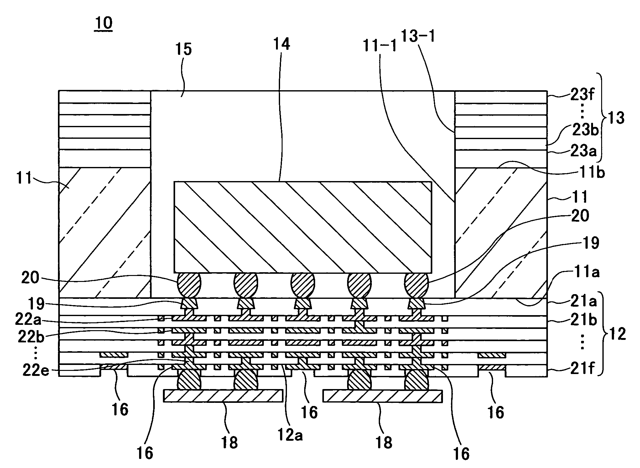
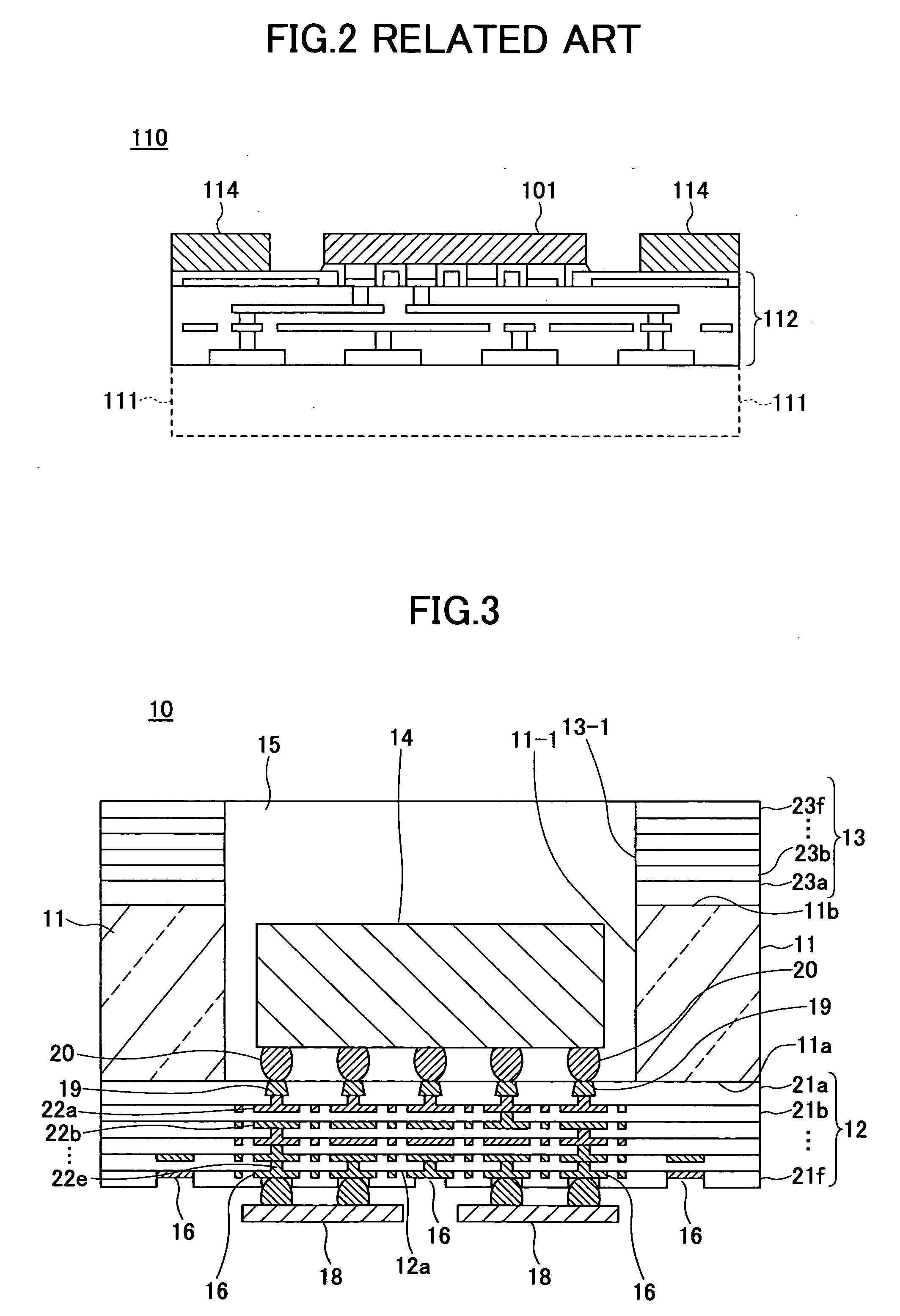
[0055]FIG. 3 is a schematic cross-sectional view of a semiconductor device of a first embodiment of the present invention.

[0056] Referring to FIG. 3, the semiconductor device 10 of the first embodiment includes a support substrate 11, a multilayer wiring layer 12, a multilayer dielectric layer 13, a semiconductor chip 14, a resin part 15, a decoupling capacitor 18, and others. The multilayer wiring layer 12 is provided at a side of a first surface 11a of the support substrate 11. The multilayer dielectric layer 13 is provided at a side of a second surface 11b of the support substrate 11. The semiconductor chip 14 is provided at opening parts 11-1 and 13-1 that pierces the support substrate 11 and the multilayer dielectric layer 13. The resin part 15 covers the semiconductor chip 14 and fills the opening parts 11-1 and 13-1. The decoupling capacitor 18 is connected to an electrode pad 16 provided at a surface 12a of the multilayer wiring layer 12. The semiconductor chip 14 is connec...

second embodiment

[0094]FIG. 10 is a schematic cross-sectional view of a semiconductor device of a second embodiment of the present invention. In the second embodiment, parts that correspond to the parts discussed in the first embodiment are given the same reference numerals in FIG. 10, and explanation thereof is omitted.

[0095] Referring to FIG. 10, a semiconductor device 40 of the second embodiment is the same as the semiconductor device of the first embodiment other than that the semiconductor device 40 includes a heat sink 41 and a stiffener 42. The heat sink 41 is provided on the semiconductor chip 14. The stiffener 42 is provided on the surface of the multilayer dielectric layer 13 so as to surround the opening part 13-1.

[0096] The heat sink 41 is made of, for example, Al, Al alloy, Cu, Cu alloy or the like having a plate configuration which has a thickness of 2 mm or a fin configuration. A high heat-conduction compound including an inorganic filler such as alumina may be applied on a contact ...


PUM


Abstract

A semiconductor device includes a support body, a first substrate provided on a surface at one side of the support body, a second substrate provided on a surface at the other side of the support body, and a semiconductor chip provided on the first substrate exposed to an opening part piercing the support body and the second substrate. The first substrate includes a first dielectric layer and a wiring layer, a plurality of first electrodes connected to the semiconductor chip which first electrodes are provided on a first surface of the first substrate exposed to an inside of the opening part, and the second substrate includes a second dielectric layer made of a material substantially the same as the first dielectric layer.

Description

CROSS-REFERNCE TO RELATED APPLICATIONS [0001] This patent application is based upon and claims the benefit of priority from the prior Japanese Patent Application No. 2004-245511 filed on Aug. 25, 2004, the entire contents of which are hereby incorporated by reference. BACKGROUND OF THE INVENTION [0002] 1. Field of the Invention [0003] The present invention relates to a semiconductor device having a multilayer printed wiring board where a semiconductor chip is provided and a manufacturing method of the same. [0004] 2. Description of the Related Art [0005] Recently and continuing, as performance and function of large scale integrated circuits (LSI) are becoming high, it is desired that mounting substrates have small size, high density and a large number of pins. A built-up multilayer substrate wherein wiring layers and dielectric layers are reciprocally stacked is being utilized as a high density mounting substrate. [0006] The built-up multilayer substrate is formed by repeating proce...

Claims


Application Information

Patent Timeline
IPC IPC(8): H01L21/48H01L23/04
CPCH01L21/4857H01L2224/16235H01L23/36H01L23/49833H01L23/5389H01L2224/16H01L2924/01046H01L2924/01078H01L2924/01079H01L2924/15153H01L2924/1517H01L2924/15312H01L2924/19105H01L2924/19106H01L2924/3011H01L2924/3511H01L2924/01019H01L2224/16225H01L2224/73253H01L23/13
Inventor ABE, TOMOYUKITANI, MOTOAKI
Owner FUJITSU LTD
Why Eureka
Try Eureka