Method of manufacturing a semiconductor device

Active Publication Date: 2006-03-02
RENESAS ELECTRONICS CORP
View PDF8 Cites 6 Cited by
  • Summary
  • Abstract
  • Description
  • Claims
  • Application Information

AI Technical Summary

Benefits of technology

[0024] When extruding a molded body in the bottom face of a mold cavity corresponding to the surface of a molded body by the pin which performs advance-or-retreat movement at the projecting portion which projects from the bottom face after forming a molded body, forming a depressed portion by the projecting portion on the surface of a molded body, it can extrude. When accumulating molded bodies in the baking step after a resin molding step and per

Problems solved by technology

Although baking treatment for promoting cure of the resin of a molded body further was performed after the resin molding step, the present inventors found out especially that the problem about poor quality occurred under the effect of the resin burr in the baking step after a resin molding step in the thin semiconductor device.
Since the length of the resin burr comes out scatteringly, the clearance also becomes uneven size for every semiconductor device.
If bake is performed in the condition that the clearan

Method used


Image

  • Method of manufacturing a semiconductor device
  • Method of manufacturing a semiconductor device
  • Method of manufacturing a semiconductor device

Examples


embodiment

(Embodiment)

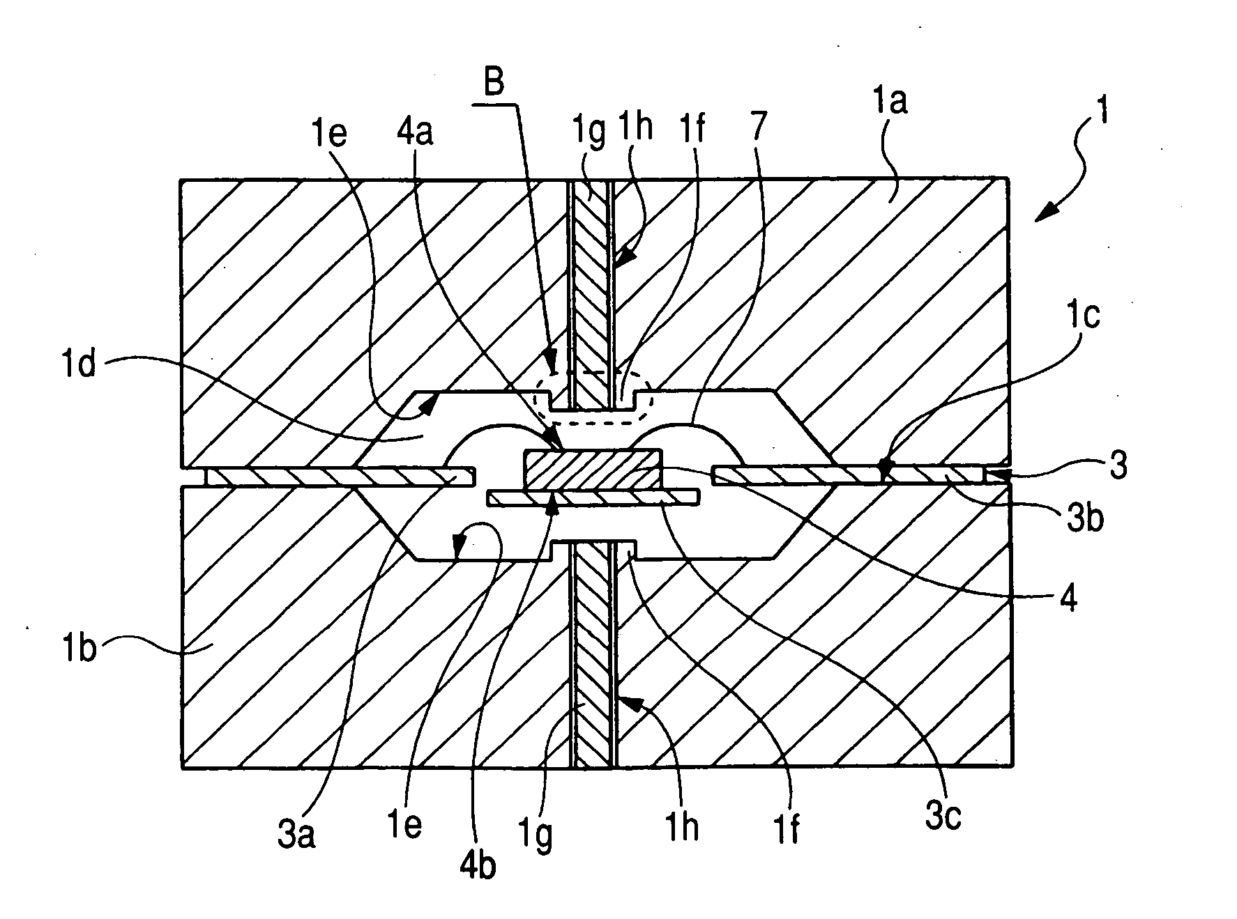
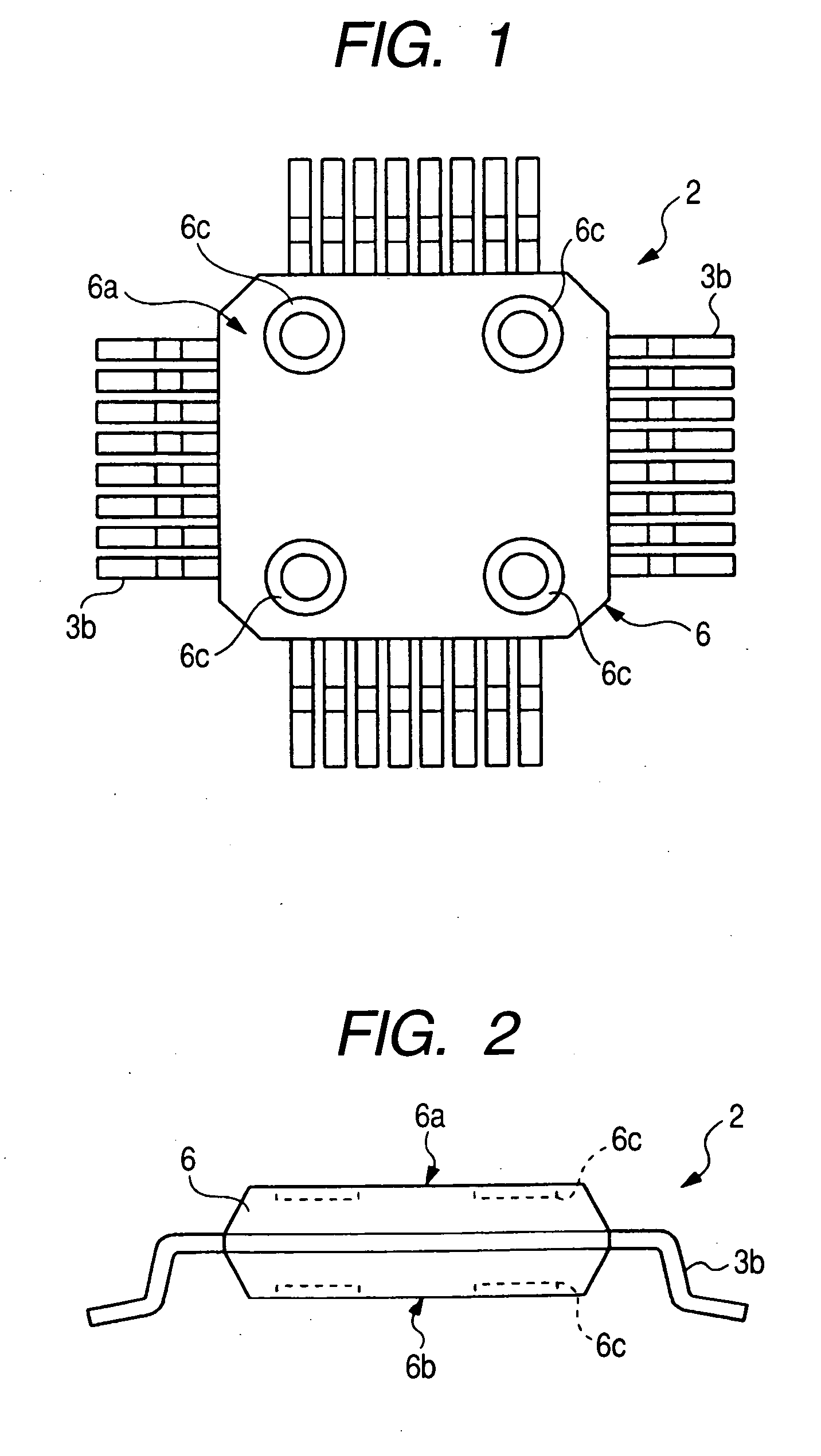
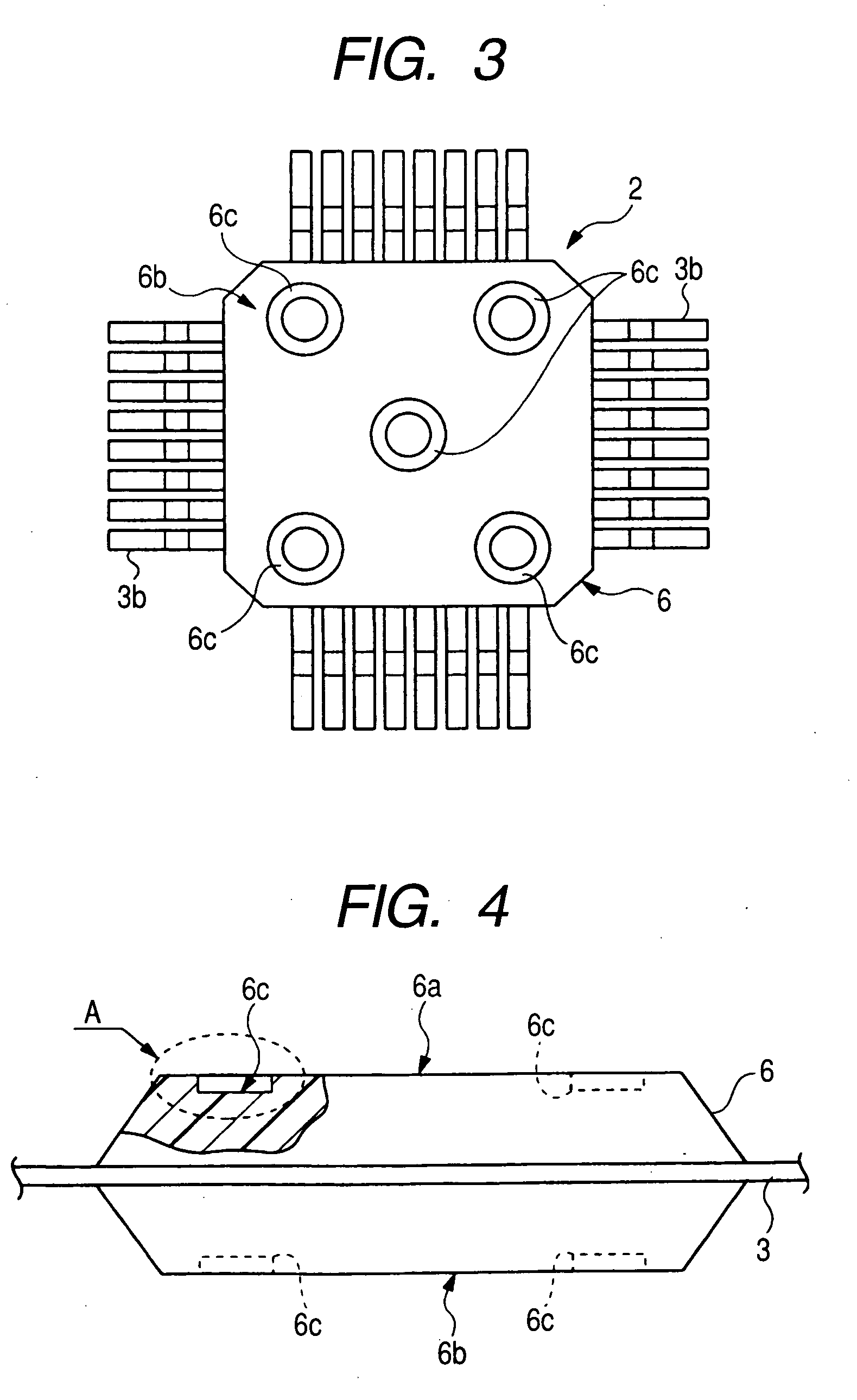
[0053]FIG. 1 is a plan view showing an example of the configuration of the semiconductor device of Embodiment of the invention; FIG. 2 is a side view showing an example of the configuration of the semiconductor device shown in FIG. 1; FIG. 3 is a back view showing an example of the configuration of the semiconductor device shown in FIG. 1; FIG. 4 is an enlarged partial side view fracturing the part of and showing the configuration of the semiconductor device shown in FIG. 1; FIG. 5 is an enlarged partial sectional view showing the configuration of the A section of FIG. 4; FIG. 6 is a sectional view showing an example of the configuration at the time of the metal-mold clamp in the resin molding step of the assembly of the semiconductor device shown in FIG. 1; FIG. 7 is an enlarged partial sectional view showing the configuration of the B section of FIG. 6; FIG. 8 is a sectional view showing an example of the configuration at the time of the resin injection in the resin mo...


PUM

PropertyMeasurementUnit
Thicknessaaaaaaaaaa
Depthaaaaaaaaaa
Particle diameteraaaaaaaaaa

Abstract

Improvement in the yield of a semiconductor device is aimed at. When extruding a molded body with the ejector pin which performs advance-or-retreat movement at the projecting portion which projects from this bottom face in the bottom face of a mold cavity corresponding to the surface and the mounting side of a molded body after forming a molded body, depressed portions being formed in the surface and the mounting side by projecting portions, they can extrude. When accumulating molded bodies themselves in the baking step after a resin molding step and performing bake, by arranging the resin burr which furthermore withdrew from the surface and the mounting side in the depressed portion, bake can be performed in the condition that the accumulated molded bodies are stuck. Therefore, the form of deformation of a warp etc. of each molded body or a lead frame, can be made uniform, and, as a result, improvement in the yield of QFP (semiconductor device) is aimed at.

Description

CROSS-REFERENCE TO RELATED APPLICATION [0001] The present application claims priority from Japanese patent application No. 2004-252108 filed on Aug. 31, 2004, the content of which is hereby incorporated by reference into this application. [0002] 1. Field of the Invention [0003] The present invention relates to a semiconductor manufacturing technology, and particularly relates to an effective technology in the application to improvement in the yield of the semiconductor device of a plastic molded type. [0004] 2. Description of the Background Art [0005] With conventional electronic parts and a resin molding device, by locating so that a rising part may be formed in a mold cavity inner surface and it may become flush with a flat face at the withdrawing and incoming point about a pin at the rising part, even if a resin burr occurs in a sheath resin part, electronic parts can be mounted on a printed circuit board in the good condition (for example, refer to Patent Reference 1). [0006] [P...

Claims


Application Information

Patent Timeline
IPC IPC(8): B29C70/70B29C70/88
CPCB29C70/84B29L2031/3406H01L2224/48091H01L2224/48247H01L2924/1815H01L2224/45144H01L2924/00014H01L2924/00
Inventor KURATOMI, BUNSHINISHITA, TAKAFUMIKAWATA, YOUICHI
Owner RENESAS ELECTRONICS CORP
Why Eureka
Try Eureka