

Low switching frequency power factor correction circuit
- Summary
- Abstract
- Description
- Claims
- Application Information
AI Technical Summary
Benefits of technology
Problems solved by technology
Method used
Image

Examples
Embodiment Construction
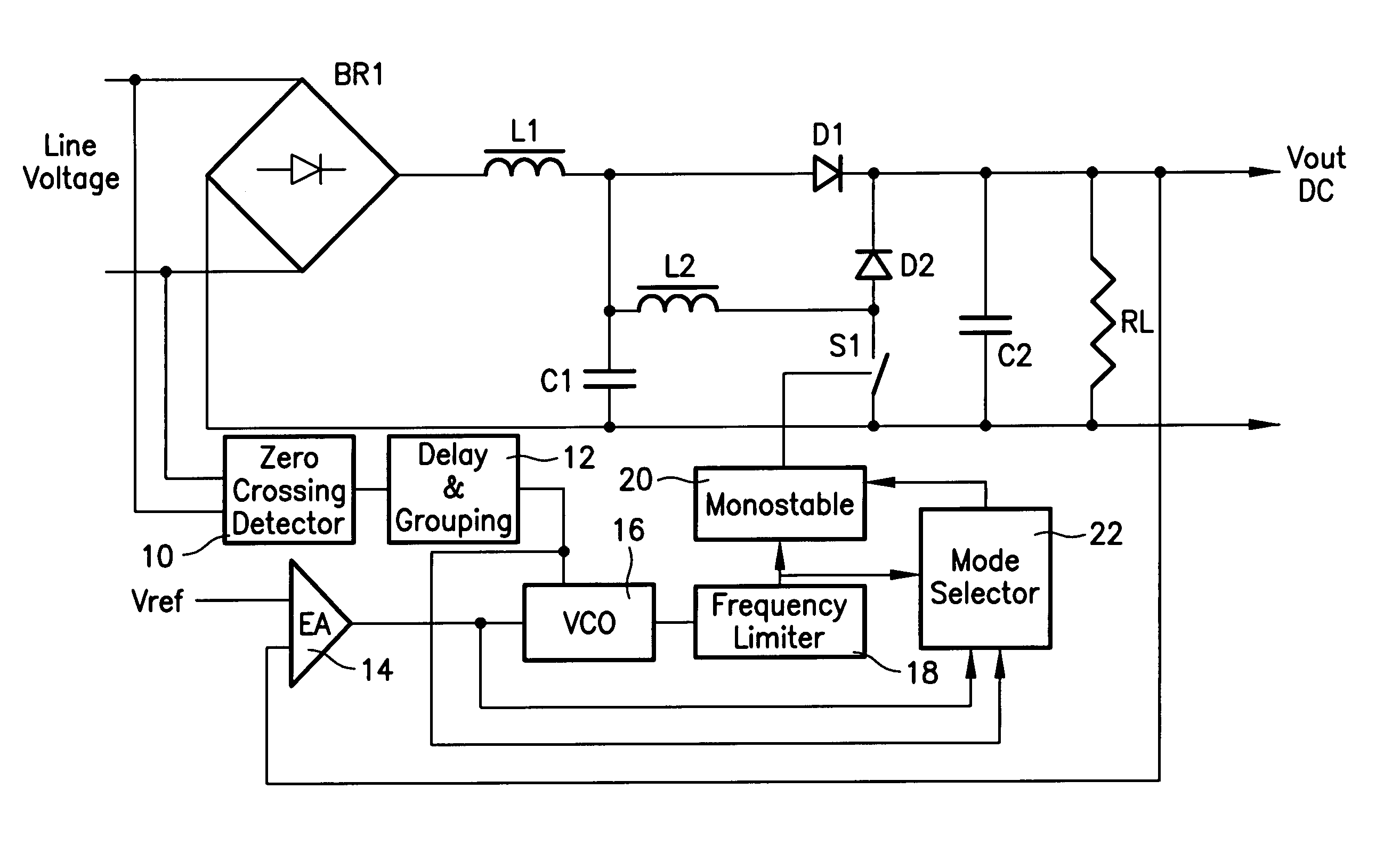
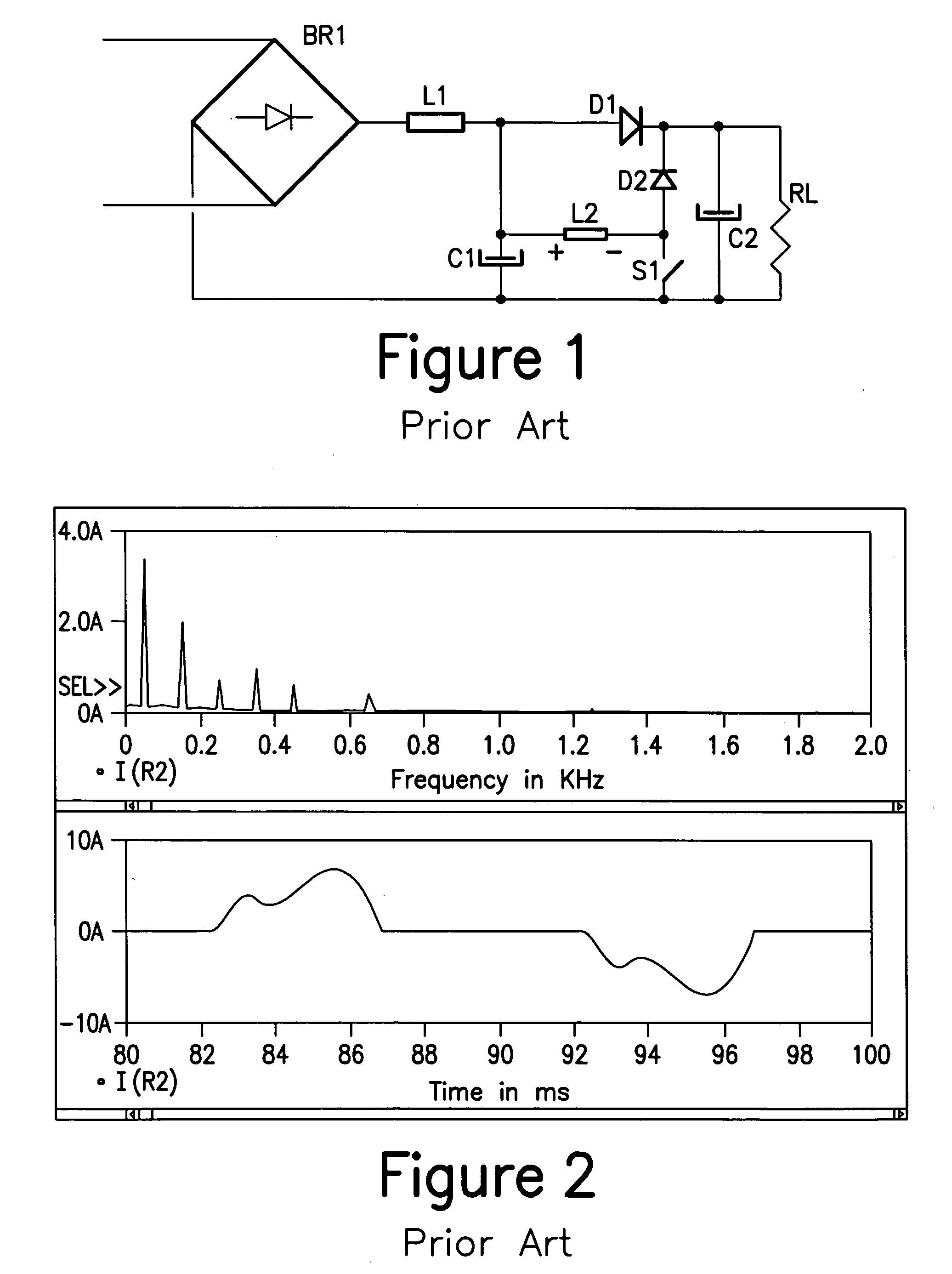
[0037] In FIG. 1, which is a prior art circuit, RL represents the equipment to be fed (very often a further power conversion stage) as the “equivalent” load to the harmonic correction (or power factor correction) circuit. The harmonic correction circuit comprises L1,C1,L2,S1, D1 and D2, while C2, together with BR1, represent the standard rectifying and filtering stage which, alone, would produce substantial distortion of the line current. In FIG. 1, the housekeeping power supply is not shown.
[0038] Referring to FIG. 1, it is clear that the circuit of FIG. 1 has several “degree of freedom” with respect to how the switch S1 can be driven ON and OFF during each line half-period.
[0039] Firstly, the modulation of switch S1 has to be the same for subsequent line half periods. In-fact, if it were different between two subsequent half line periods, the line current would become rich in even harmonics, whose regulation limits are much more stringent than for odd harmonics.
[0040] Given thi...
PUM
 Abstract
Description
Claims
Application Information