Method for forming individual semi-conductor devices

a technology of semiconductor devices and semiconductor chips, applied in the direction of instruments, furnaces, forging furnaces, etc., can solve the problems of vibration or impact, easy damage to mechanical elements, etc., and achieve the effect of suppressing damage to the mechanical element of mems chips

Inactive Publication Date: 2006-03-02
LAPIS SEMICON CO LTD
View PDF4 Cites 7 Cited by
  • Summary
  • Abstract
  • Description
  • Claims
  • Application Information

AI Technical Summary

Benefits of technology

[0011] According to the present invention, a semiconductor substrate located in the position in forming individual semiconductor devices, which corresponds to a scribe line as a cutting region, is thinned from the face (first face) where the scribe line is formed. Accordingly, it is possible to cut the semiconductor substrate in a non-contact cutting manner by using an instrument such as a laser. Therefore, it is possible to suppress damage to the mechanical element of MEMS chips due to an external force applied while cutting.

Problems solved by technology

Since a mechanical element included in an MEMS chip is very fragile with regards to external vibration and impact, in a dicing process where individual MEMSs are formed, the mechanical elements are easily damaged due to the mechanical vibration or impact from cleaning water spray.
Accordingly, it is inevitable that vibrations or an impact occurs when cutting.

Method used


Image

  • Method for forming individual semi-conductor devices
  • Method for forming individual semi-conductor devices
  • Method for forming individual semi-conductor devices

Examples


first embodiment

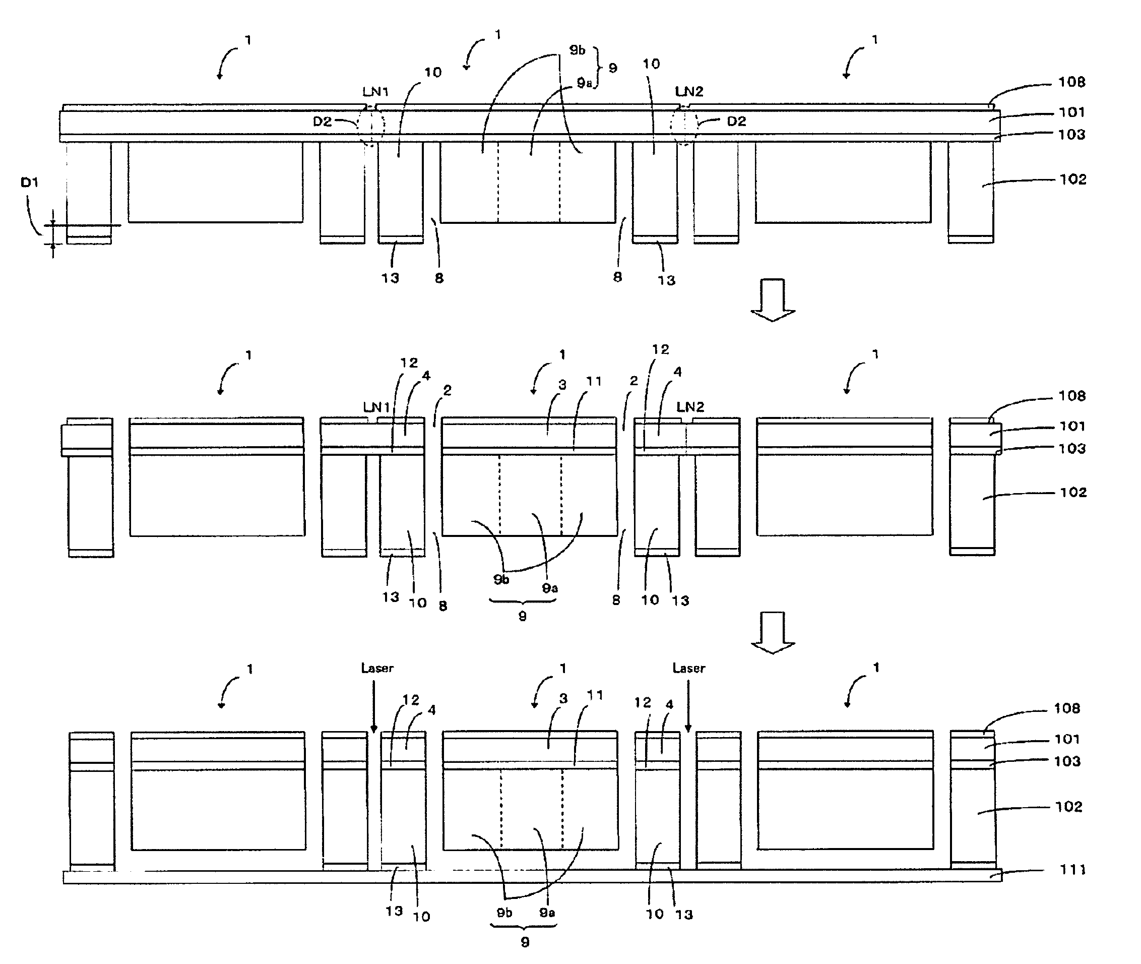
[0020] Referring to a method for forming individual semiconductor devices (MEMSs) according to a first embodiment of the present invention, an exemplary piezoresistance type acceleration sensing device 1 produced by using an SOI substrate is described.

Structure

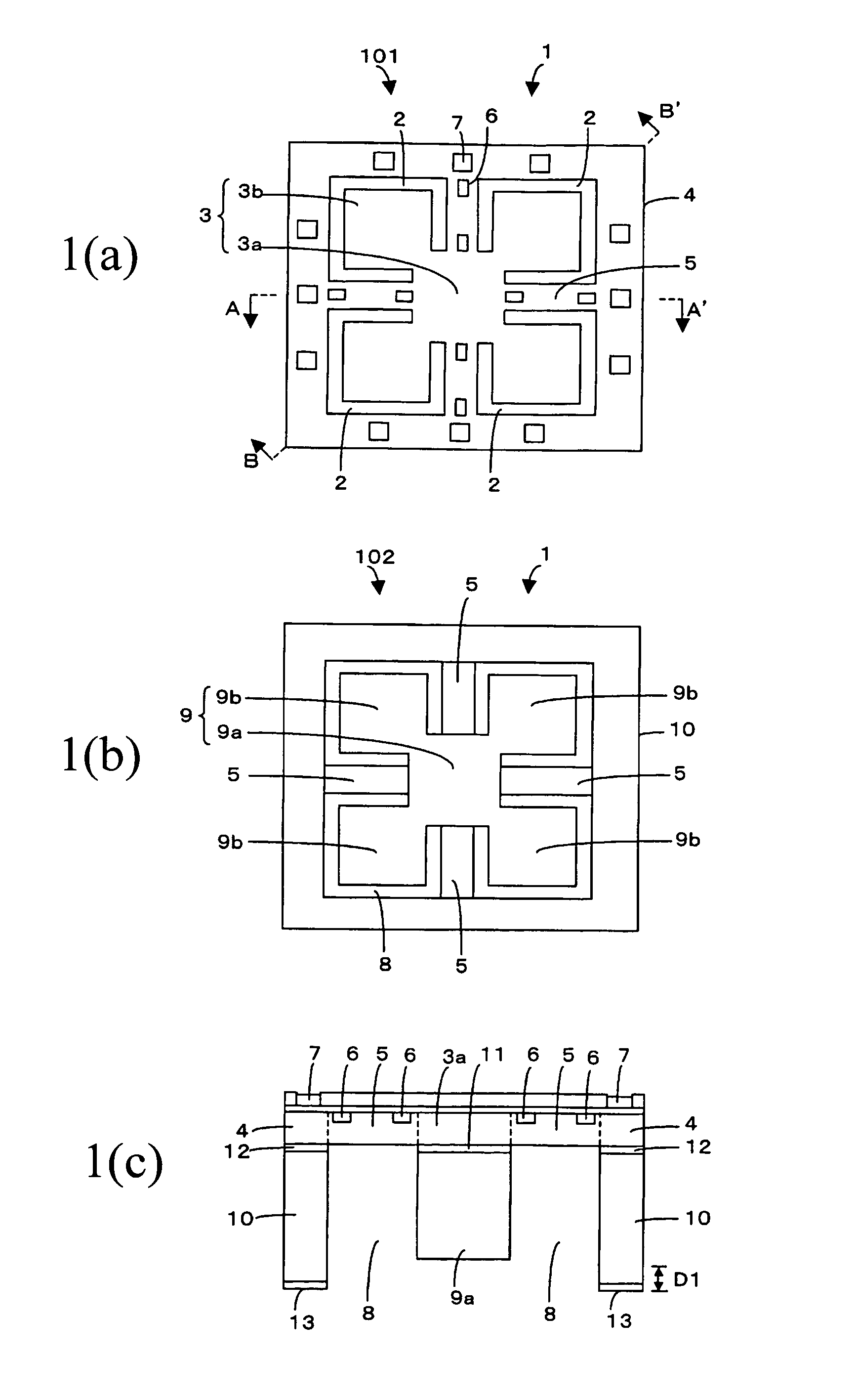
[0021] FIGS. 1(a) to 1(c) show structural views of the piezoresistance type acceleration sensing device 1 produced by using the SOI substrate. FIG. 1(a) shows a plan view of the acceleration sensing device 1. FIG. 1(b) shows a bottom view thereof. FIG. 1(c) shows a cross-sectional view taken along a line A-A′ of FIG. 1(a).

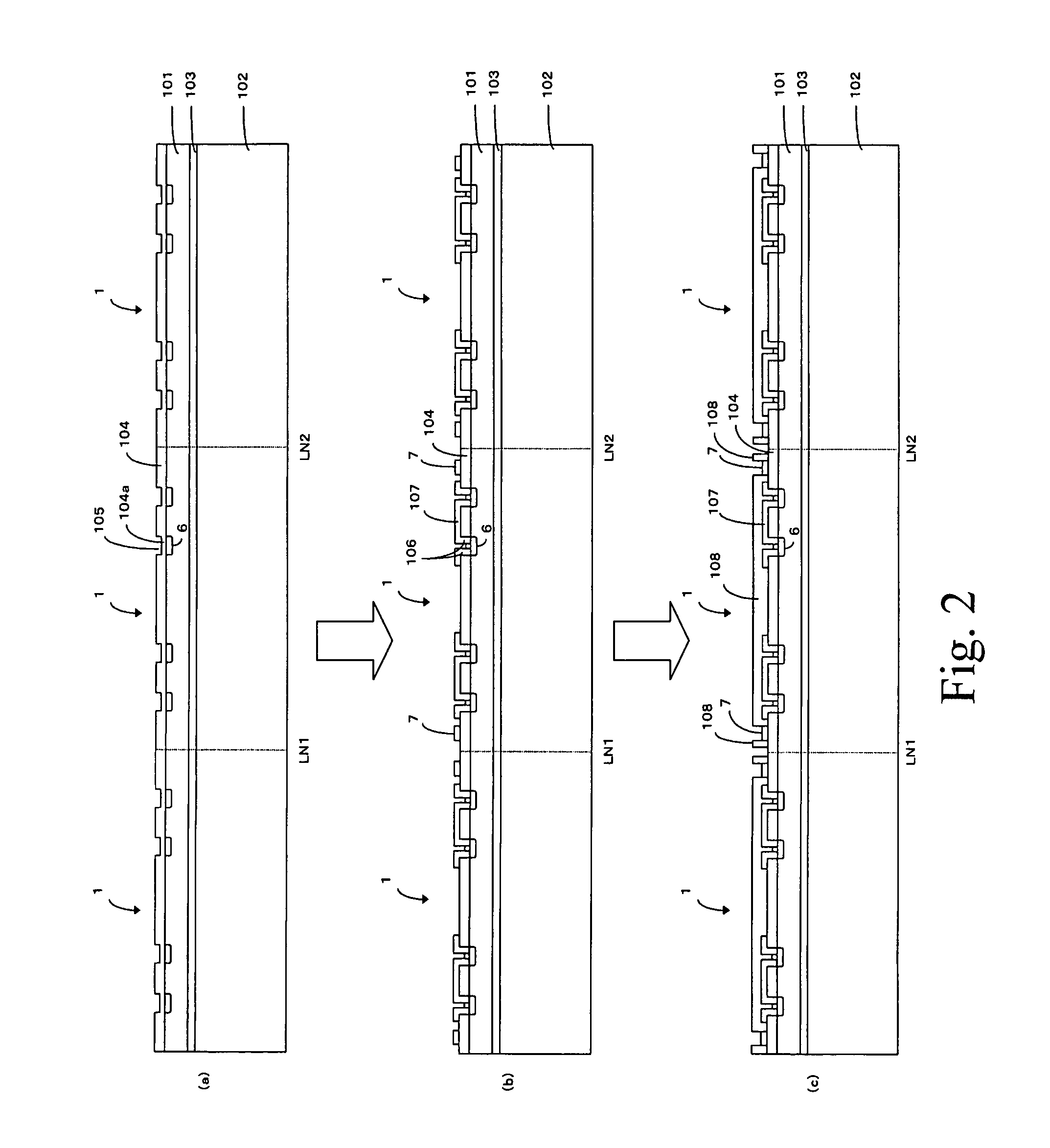
[0022] As shown in line (a) of FIG. 2, the SOI substrate is a semiconductor substrate that includes a buried oxide film 103 provided with a first Si film 101 and a second Si film 102 formed on opposing sides of the buried oxide film 103. As shown in FIG. 1(a), the first Si film 101 is divided by dividing grooves 2 on a first face, thus, a mass portion 3, a support portion 4, and beam portions 5 are formed...

second embodiment

[0043] A second embodiment will now be explained. In view of the similarity between the first and second embodiments, the parts of the second embodiment that are identical to the parts of the first embodiment will be given the same reference numerals as the parts of the first embodiment. Moreover, the descriptions of the parts of the second embodiment that are identical to the parts of the first embodiment may be omitted for the sake of brevity.

[0044] In a second embodiment, although the scribe lines are thinned in a manner similar to the first embodiment, the scribe lines are additionally cut in a part of manufacturing processes of MEMS chips (acceleration sensing device).

Structure

[0045] The structure of the second embodiment is similar or identical to the acceleration sensing device 1 of the first embodiment shown in FIGS. 1(a) to (c).

Method for Manufacturing Device and Forming Individual Devices

Forming Electric Element

[0046] Similar to the first embodiment, the electric ...


PUM

PropertyMeasurementUnit
temperaturesaaaaaaaaaa
thicknessaaaaaaaaaa
thickness D1aaaaaaaaaa

Abstract

The present invention provides a method that forms individual semiconductor devices from a semiconductor substrate including a first face having a first region in which micro-mechanical elements are formed and a second region which surrounds the first region and in which a scribe line is formed, and a second face having a third region which is opposed to the first face and corresponds to the first region in which the micro-mechanical elements are formed and a fourth region which surrounds the third region and corresponds to the second region. The method includes steps of thinning the fourth region of the second face which corresponds to the scribe line formed in the second region of the first face, and cutting the semiconductor substrate along the scribe line formed in the second region of the first face.

Description

BACKGROUND OF THE INVENTION [0001] 1. Field of the Invention [0002] The present invention generally relates to a method for forming semiconductor devices. More specifically, the present invention relates to a method for forming individual semiconductor devices including micro-mechanical elements formed on a semiconductor substrate, also known as MEMS (Micro Electro Mechanical System) chips. [0003] 2. Background Information [0004] MEMS is a system by which very small micro-mechanical elements and electronic circuits are integrated on a semiconductor substrate by using ultra-fine processing technology for the semiconductor. MEMS chips are mechanically cut by a diamond cutter when they are separated into individual chips, in a process that is generally similar to those of typical semiconductor devices. [0005] A method for forming individual semiconductor devices is disclosed in Japanese Laid-Open Patent Publication TOKUKAI No. JP2001-144035 (especially page 3-4, FIGS. 1 and 2), for exa...

Claims


Application Information

Patent Timeline
Patent Type & Authority Applications(United States)
IPC IPC(8): H01L21/78H01L21/301
CPCB81C1/00873B21J13/08B21J17/00
Inventor OZAWA, NOBUO
Owner LAPIS SEMICON CO LTD
Why Eureka
Try Eureka