Method for integrated circuit fabrication using pitch multiplication

a technology of integrated circuits and multiplication, applied in the field of masking techniques, can solve the problems of inability to reliably use photolithographic techniques, the flexibility required to define circuits will typically not be possible using a single mask, and the inability to achieve the effect of defining circuits

Inactive Publication Date: 2006-03-02
ROUND ROCK RES LLC
View PDF32 Cites 531 Cited by
  • Summary
  • Abstract
  • Description
  • Claims
  • Application Information

AI Technical Summary

Benefits of technology

[0021] According to another aspect of the invention, a process is provided for fabricating an integrated circuit. The process comprises providing a masking layer extending over a first and a second region of a partially fabricated integrated circuit. A pattern is formed in the masking layer. A minimum feature size of a portion of the pattern corresponding to the first region is equal to or less than about half a minimum feature size of an other portion of the pattern corresponding to the second region.
[0022] According to another aspect of the invention, a partially formed integrated circuit is provided. The partially formed integrated circuit comprises a carbon layer and a plurality of pitch-multiplied spacers on a level overlying the carbon layer. The spacers have a pitch of about 100 nm or less.

Problems solved by technology

Due to factors such as optics and light or radiation wavelength, however, photolithography techniques each have a minimum pitch below which a particular photolithographic technique cannot reliably form features.
Moreover, even if peripheral features can be formed with the same pitch as the array, the flexibility required to define circuits will typically not be possible using a single mask, particularly if the patterns are limited to those that can be formed along the sidewalls of patterned photoresist.
Because such methods form patterns using different masks at different locations on a substrate, they are limited in their ability to form features that require overlapping patterns, such as when a landing pad overlaps an interconnect line, and yet a third mask may be necessitated to “stitch” two separate patterns with interconnects.
Additionally, such a third mask would face even greater challenges with respect to mask alignment due to the fine features defined by the pitch multiplication technique.

Method used


Image

  • Method for integrated circuit fabrication using pitch multiplication
  • Method for integrated circuit fabrication using pitch multiplication
  • Method for integrated circuit fabrication using pitch multiplication

Examples


Embodiment Construction

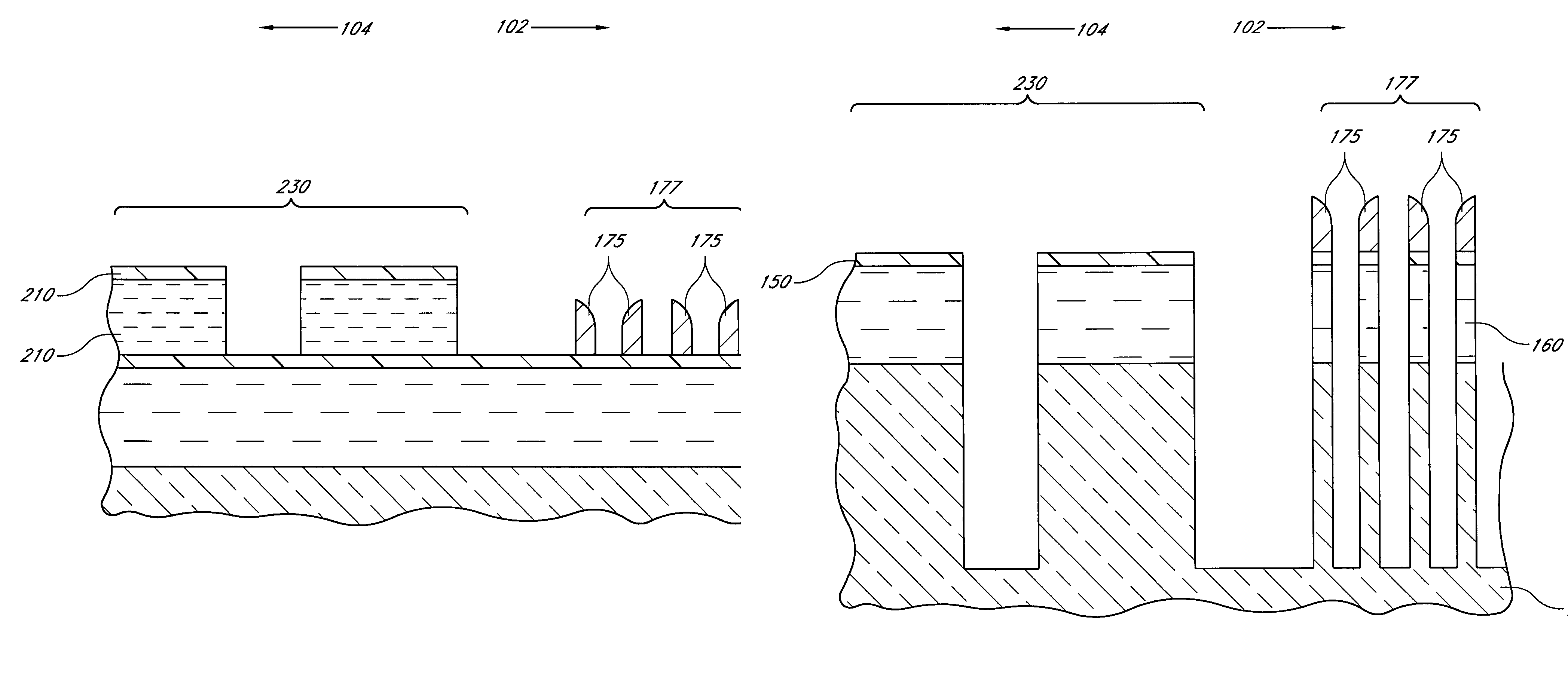
[0042] In addition to problems with forming different size features, it has been found that pitch doubling techniques can have difficulty transferring spacer patterns to a substrate. In particular, in common methods of transferring patterns, both the spacers and the underlying substrate are exposed to an etchant, which preferentially etches away the substrate material. It will be appreciated, however, that the etchants also wear away the spacers, albeit at a slower rate. Thus, over the course of transferring a pattern, the spacers can be worn away by the etchant before the pattern transfer is complete. These difficulties are exacerbated by the trend towards decreasing feature size, which, for example, increasingly leads to higher aspect ratios as the widths of these trenches decrease. In conjunction with difficulties of producing structures of different feature sizes, these pattern transfer limitations make even more difficult the application of pitch-doubling principles to integrat...


PUM


Abstract

Different sized features in the array and in the periphery of an integrated circuit are patterned on a substrate in a single step. In particular, a mixed pattern, combining two separately formed patterns, is formed on a single mask layer and then transferred to the underlying substrate. The first of the separately formed patterns is formed by pitch multiplication and the second of the separately formed patterns is formed by conventional photolithography. The first of the separately formed patterns includes lines that are below the resolution of the photolithographic process used to form the second of the separately formed patterns. These lines are made by forming a pattern on photoresist and then etching that pattern into an amorphous carbon layer. Sidewall pacers having widths less than the widths of the un-etched parts of the amorphous carbon are formed on the sidewalls of the amorphous carbon. The amorphous carbon is then removed, leaving behind the sidewall spacers as a mask pattern. Thus, the spacers form a mask having feature sizes less than the resolution of the photolithography process used to form the pattern on the photoresist. A protective material is deposited around the spacers. The spacers are further protected using a hard mask and then photoresist is formed and patterned over the hard mask. The photoresist pattern is transferred through the hard mask to the protective material. The pattern made out by the spacers and the temporary material is then transferred to an underlying amorphous carbon hard mask layer. The pattern, having features of difference sizes, is then transferred to the underlying substrate.

Description

REFERENCE TO RELATED APPLICATIONS [0001] This application is related to the following: U.S. patent application Ser. No. ______ to Abatchev et al., filed Aug. 31, 2004, entitled Critical Dimension Control, Attorney Docket No. MICRON.286A (Micron Ref. No. 03-1348.00 / US); U.S. patent application Ser. No. ______ to Abatchev et al., filed Sep. 1, 2004, entitled Mask Material Conversion, Attorney Docket No. MICRON.293A (Micron Ref. No. 03-1435.00 / US); U.S. patent application Ser. No. ______ to Tran et al., filed Aug. 31, 2004, entitled Methods for Increasing Photo-Alignment Margins, Attorney Docket No. MICRON.295A (Micron Ref. No. 04-0068.00 / US); and U.S. patent application Ser. No. ______ to Sandhu et al., filed Sep. 2, 2004, entitled Methods to Align Mask Patterns, Attorney Docket No. MICRON.296A (Micron Ref. No. 04-0114.00 / US).BACKGROUND OF THE INVENTION [0002] 1. Field of the Invention [0003] This invention relates generally to integrated circuit fabrication and, more particularly, to...

Claims


Application Information

Patent Timeline
Patent Type & Authority Applications(United States)
IPC IPC(8): H01L21/302H01L21/461
CPCH01L21/0332H01L21/0337H01L21/0338H01L21/32139H01L21/3086H01L21/3088H01L21/31144H01L21/3081Y10S438/947Y10S438/95H01J37/3174
Inventor ABATCHEV, MIRZAFER K.SANDHU, GURTEJTRAN, LUANRERICHA, WILLIAM T.DURCAN, D. MARK
Owner ROUND ROCK RES LLC
Why Eureka
Try Eureka