Microfabricated chip and method of use
- Summary
- Abstract
- Description
- Claims
- Application Information
AI Technical Summary
Benefits of technology
Problems solved by technology
Method used
Image

Examples
Embodiment Construction
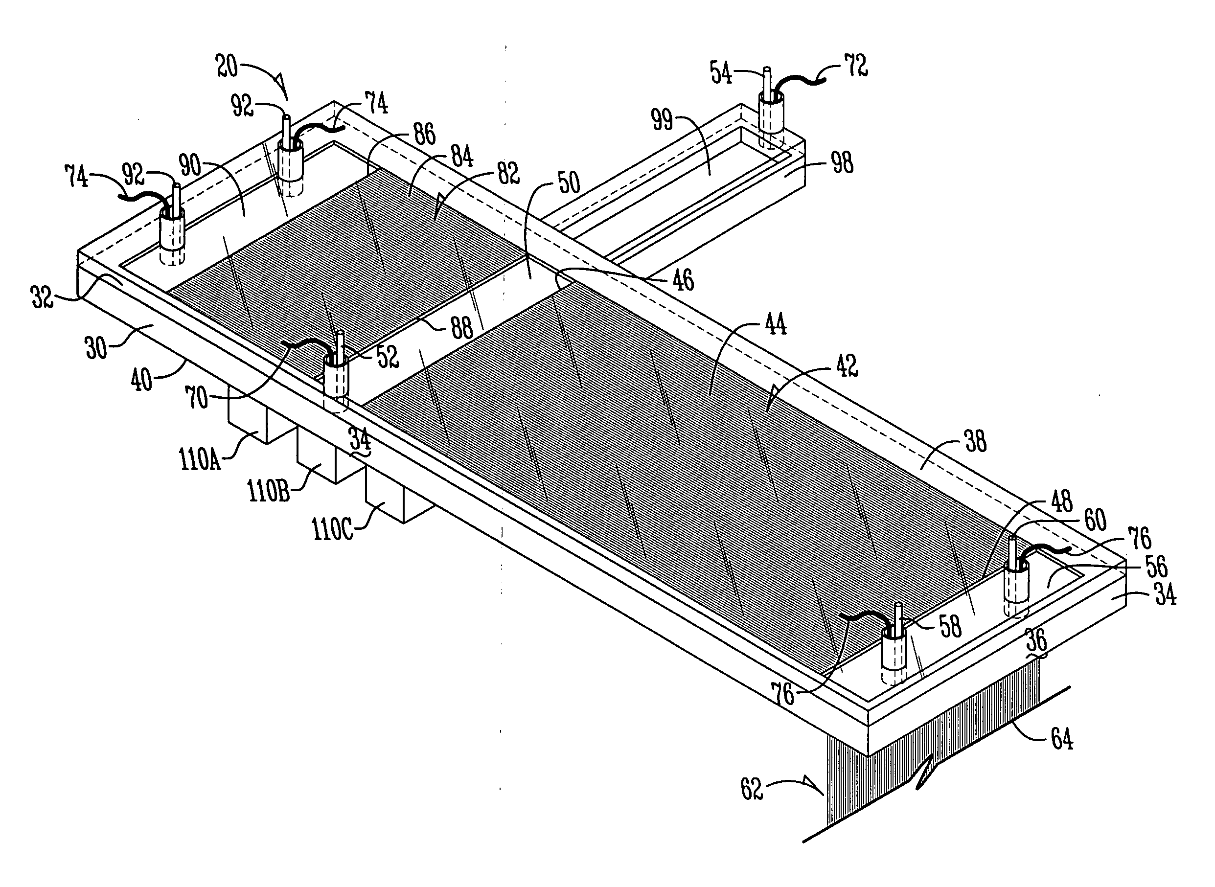
[0029] The invention, as hereinbefore explained, is a microfabricated chip in use with a multiplexed, absorbance-based electrophoresis system. The invention system and method are for the separation, detection and identification of protein species.
[0030] By “chip” the applicants mean a discrete piece of material processed to have specialized electrical, chemical, and / or mechanical characteristics upon a plurality of samples. By “microfabricated” the applicants refer to structural elements or features of a device, which have at least one fabricated dimension in the range of from about 0.1 μm to about 500 μm.
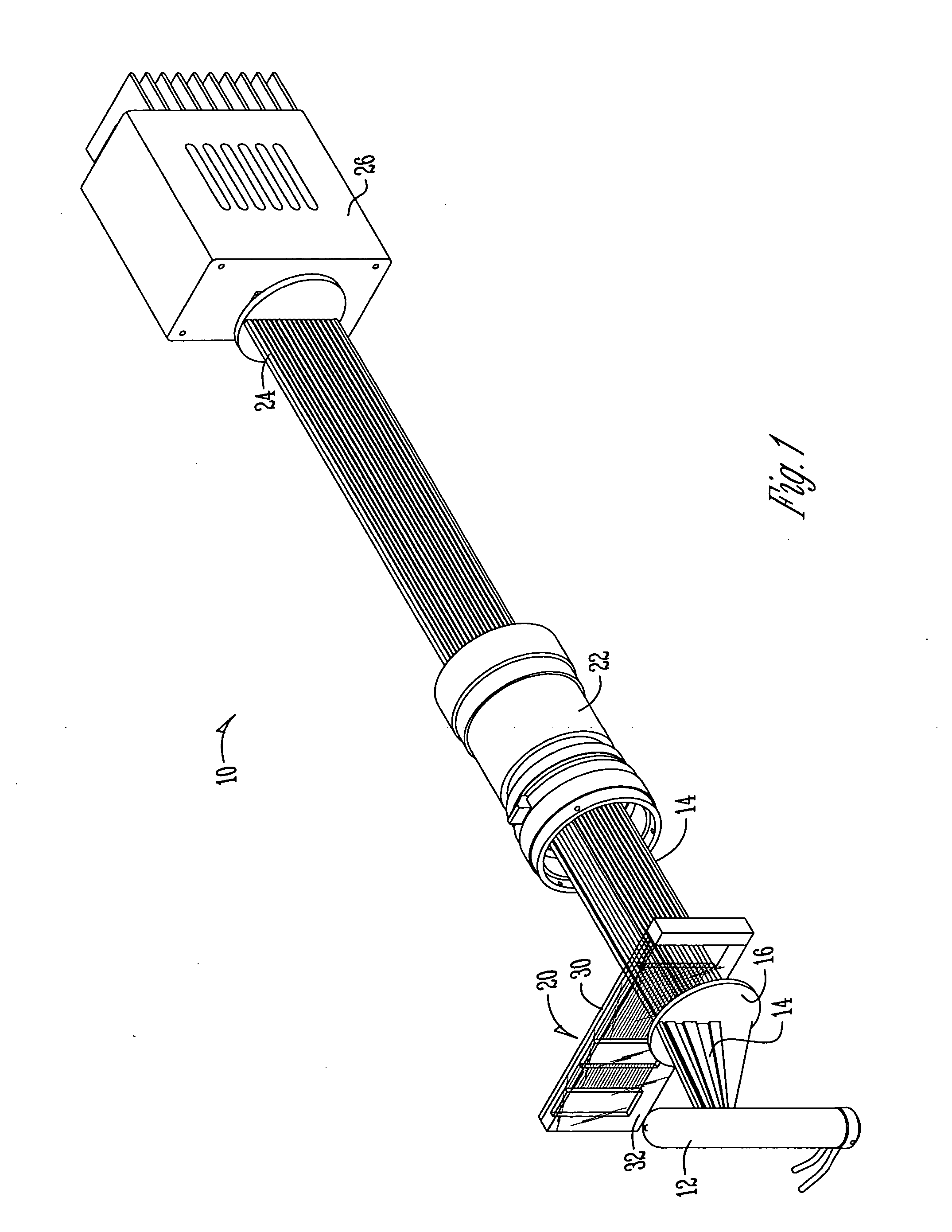
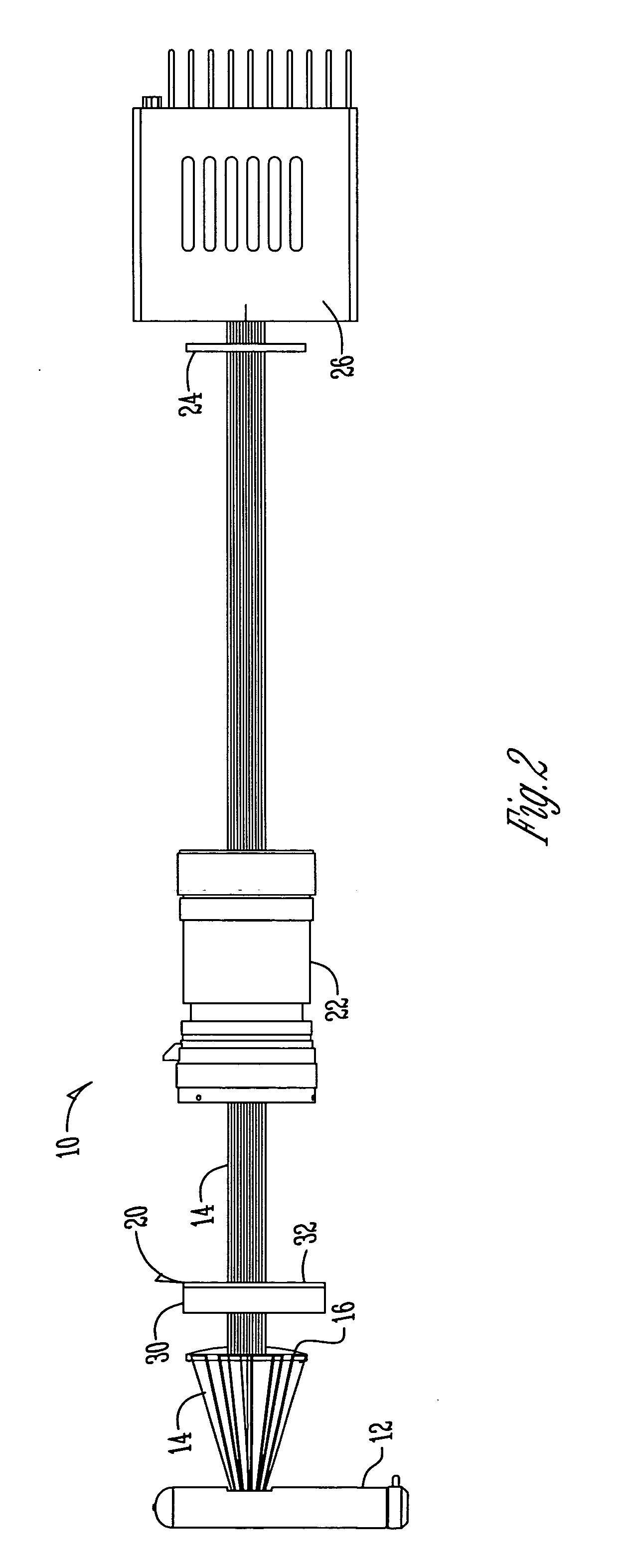
[0031] Referring to FIG. 1 and FIG. 2, numeral 10 designates the absorbance-based electrophoresis system. The light beam 14 originates in the light source 12 and then travels through the collimating lens 16, the microfabricated chip 20, the flat-field lens 22, the optical filter 24 and is collected in the detector 26.
[0032] The distance between the area where light is emitted fr...
PUM
| Property | Measurement | Unit |
|---|---|---|
| Length | aaaaa | aaaaa |
| Length | aaaaa | aaaaa |
| Length | aaaaa | aaaaa |
Abstract
Description
Claims
Application Information
 - R&D Engineer
- R&D Manager
- IP Professional
- Industry Leading Data Capabilities
- Powerful AI technology
- Patent DNA Extraction
Browse by: Latest US Patents, China's latest patents, Technical Efficacy Thesaurus, Application Domain, Technology Topic.
© 2024 PatSnap. All rights reserved.Legal|Privacy policy|Modern Slavery Act Transparency Statement|Sitemap