Plasma display panel and manufacturing method thereof

a technology of plasma display panel and manufacturing method, which is applied in the manufacture of electrode systems, electric discharge tubes/lamps, instruments, etc., can solve the problems of reducing reducing reducing the size of the discharge cell. achieve the effect of improving the brightness of the plasma display panel, high resolution and ensuring the structural stability of the barrier rib

Inactive Publication Date: 2006-03-09
LG ELECTRONICS INC
View PDF7 Cites 18 Cited by
  • Summary
  • Abstract
  • Description
  • Claims
  • Application Information

AI Technical Summary

Benefits of technology

[0025] The present invention may secure the area of a discharge cell through forming a plurality of barrier rib layers with different etch rate from each other.
[0026] The present invention may improve the brightness of a plasma display panel through forming a plurality of barrier rib layers with different etch rate from each other.
[0027] The present invention may provide a discharge cell of a plasma display panel which supports the high resolution through forming a plurality of barrier rib layers with different etch rate from each other.
[0028] The present invention may secure the structural stability of the barrier rib through forming a plurality of barrier rib layers with different etch rate from each other.

Problems solved by technology

In addition, in case of the plasma display panel which supports high resolution the area of the discharge cell is decreased, so that it becomes more difficult to implement the discharge cell of the plasma display panel supporting high resolution, if the width of lower part of the barrier rib is great.
Accordingly, there is a problem that the area of the discharge cell is broaden, however, the barrier rib 21 collapses.

Method used


Image

  • Plasma display panel and manufacturing method thereof
  • Plasma display panel and manufacturing method thereof
  • Plasma display panel and manufacturing method thereof

Examples


Embodiment Construction

[0037] Preferred embodiments of the present invention will be described in a more detailed manner with reference to the drawings.

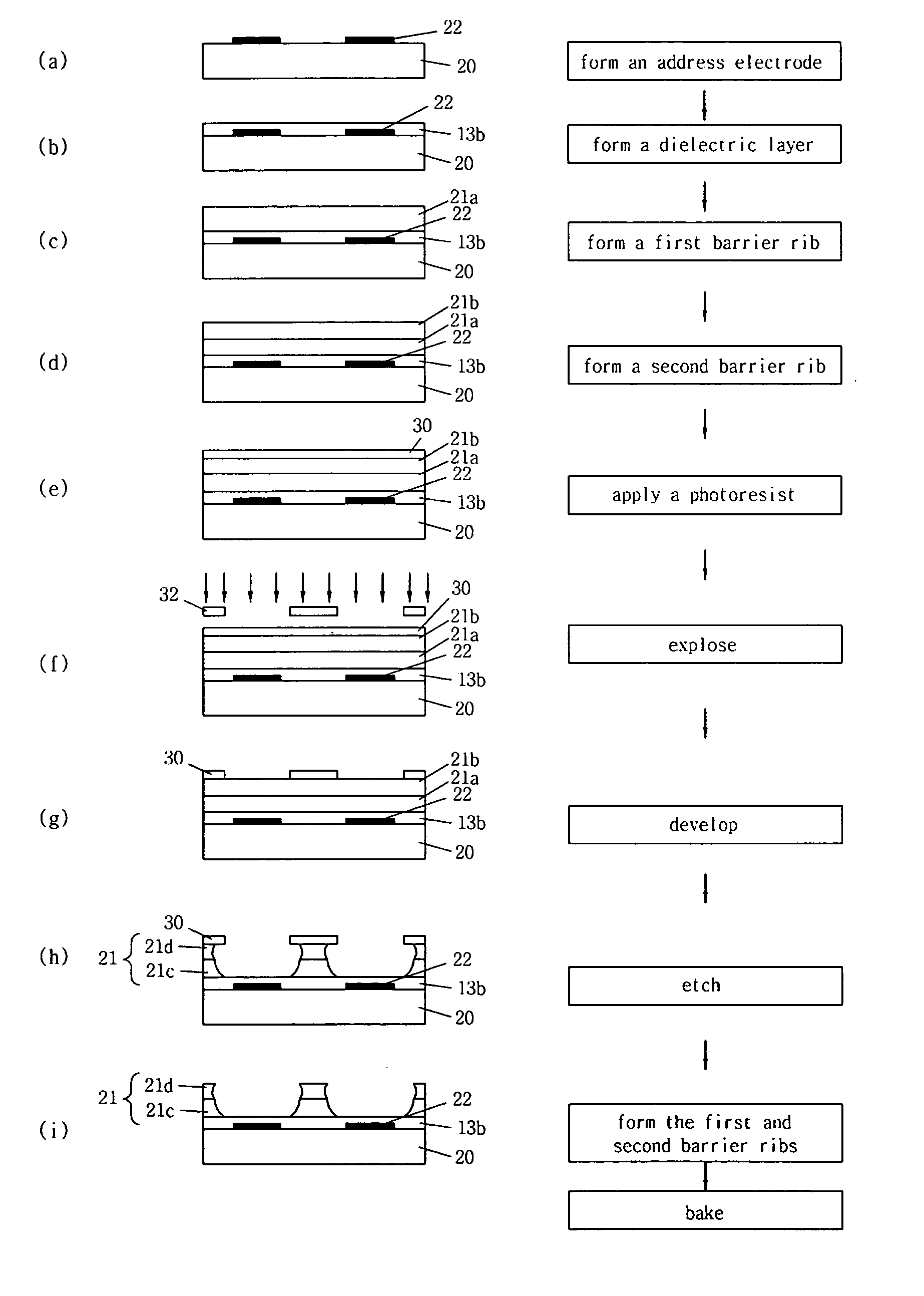
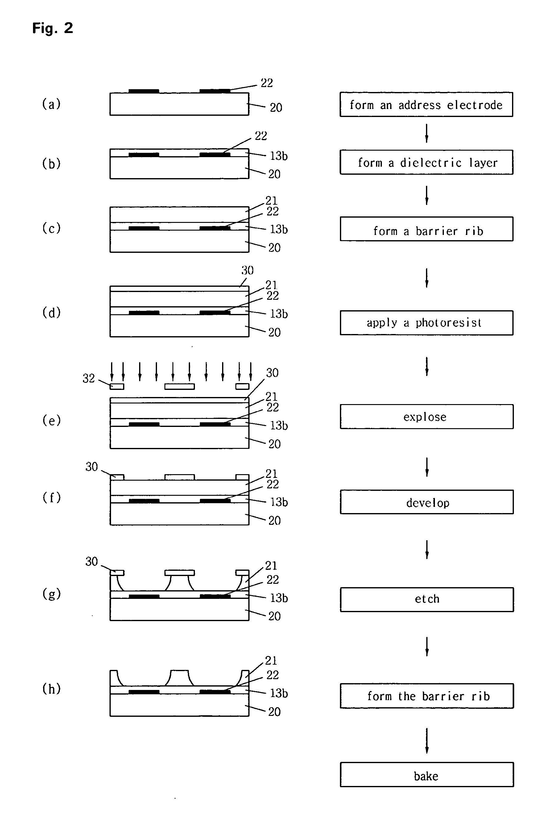
[0038] A plasma display panel according to the present invention includes a display panel, a frame formed on the rear surface of said display panel, and at least two or more thermal conductive sheets formed on a surface between said display panel and said frame, wherein said thermal conductive sheets are separated and spaced apart with a predetermined interval. A method of manufacturing the plasma display panel of the present invention includes the steps of stacking a plurality of barrier rib material layers with different etch rate from each other on a glass substrate; and forming the barrier rib through etching said plurality of barrier rib material layers with different etch rate from each other.

[0039] As becoming more distant from said glass substrate, so the barrier rib material layer with low etch rate is stacked thereon.

[0040] A method of manufac...


PUM


Abstract

The present invention relates to a plasma display panel and a manufacturing method thereof, and more particularly, to a plasma display panel including barrier ribs and a manufacturing method thereof. A method of manufacturing a plasma display panel according to the present invention comprises the steps of stacking a plurality of barrier rib material layers with different etch rate from each other on a glass substrate; and forming the barrier rib through etching said plurality of barrier rib material layers with different etch rate from each other. The present invention may secure the maximum area of the discharge cell as well as the structural stability of the barrier rib.

Description

CROSS-REFERENCES TO RELATED APPLICATIONS [0001] This Non provisional application claims priority under 35 U.S.C. § 119(a) on Patent Application No. 2004-0071469 filed in Korea on Sep. 7, 2004 the entire contents of which are hereby incorporated by reference. BACKGROUND OF THE INVENTION [0002] 1. Field of the Invention [0003] The present invention relates to a plasma display panel and a manufacturing method thereof, and more particularly, to a plasma display panel including barrier ribs and a manufacturing method thereof [0004] 2. Background of the Related Art [0005] In general, a plasma display panel is a device, where a single unit cell is composed of barrier ribs formed between a front substrate and a rear substrate made of soda-lime glass, and in each cell, vacuum ultraviolet rays are generated when inert gases such as He—Xe, He—Ne or like are discharged by a high frequency voltage, and it allows a phosphor formed within barrier ribs to radiate light, thus implementing a image. [...

Claims


Application Information

Patent Timeline
Patent Type & Authority Applications(United States)
IPC IPC(8): H01J17/49
CPCH01J9/242H01J2211/366H01J11/36H01J11/12H01J2211/363
Inventor LIM, JONG RAEKIM, WOO TAE
Owner LG ELECTRONICS INC
Why Eureka
Try Eureka