

In-situ chamber clean process to remove by-product deposits from chemical vapor etch chamber
- Summary
- Abstract
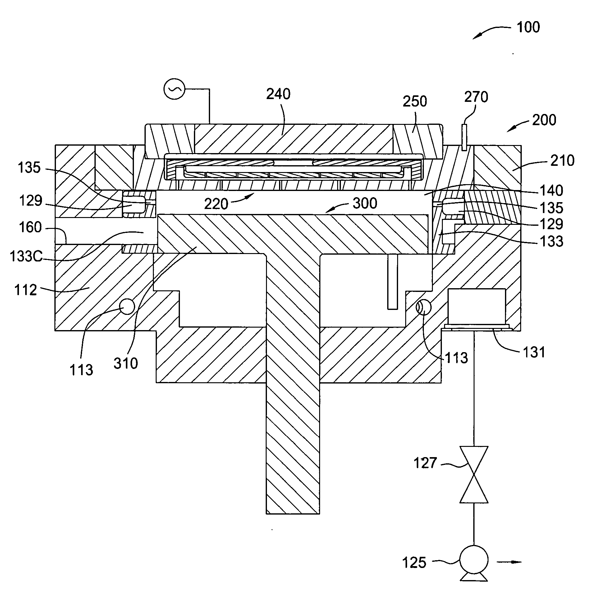
- Description
- Claims
- Application Information
AI Technical Summary
Problems solved by technology
Method used
Image

Examples
example
[0121] During etch, a gas mixture of 2 sccm of NF3, 10 sccm of NH3 and 2,500 sccm of argon was introduced into the chamber. A plasma of the gas mixture was ignited using 100 Watts of power. The bottom purge was 1,500 sccm of argon and the edge purge was 50 sccm of argon. The chamber pressure was maintained at about 6 Torr, and the substrate temperature was about 22° C. The substrate was etched for 120 seconds.
[0122] During subsequent annealing, the spacing was 750 mil and the lid temperature was 120° C. The substrate was annealed for about 60 seconds. About 50 angstroms of material was removed from the substrate surface. No anneal effect was observed. The etch rate was about 0.46 angstroms per second (28 Å / min). The observed etch uniformity was about 5% for the 50 Å etch.
[0123] The advantage of the cleaning regime includes requiring no additional processing equipment and no need to open the chamber for wet cleaning. The process also requires no constant monitoring or labor intensi...
PUM
| Property | Measurement | Unit |
|---|---|---|
| Temperature | aaaaa | aaaaa |
| Temperature | aaaaa | aaaaa |
| Temperature | aaaaa | aaaaa |
Abstract
Description
Claims
Application Information