Semiconductor circuit with mask register

Active Publication Date: 2006-03-09
LAPIS SEMICON CO LTD
View PDF4 Cites 15 Cited by
  • Summary
  • Abstract
  • Description
  • Claims
  • Application Information

AI Technical Summary

Benefits of technology

[0035] The mask register is preferably set from within the integrated circuit, so that the mask signal is not affected by the behavior of an external signal generator during the transient period while power is being shut off, and unpredictable input signals during this period are reliably masked. Moreover, even if the output of the mask register goes temporarily high during the transient period, the latch circuit does not latch the high level. The standby mode can therefore be reliably entered

Problems solved by technology

As advances in semiconductor fabrication technology continue to reduce the sizes of transistors, the current that leaks through the transistors in the off-state continues to increase, causing large-scale integrated (LSI) circuits to draw significant amounts of current even in the standby state in which their input signals, output signals, and clock signals are all halted.
This is a particularly serious problem for portable devices that operate on battery power; reducing the current consumption of these devices in the standby

Method used


Image

  • Semiconductor circuit with mask register
  • Semiconductor circuit with mask register
  • Semiconductor circuit with mask register

Examples


Example

First Embodiment

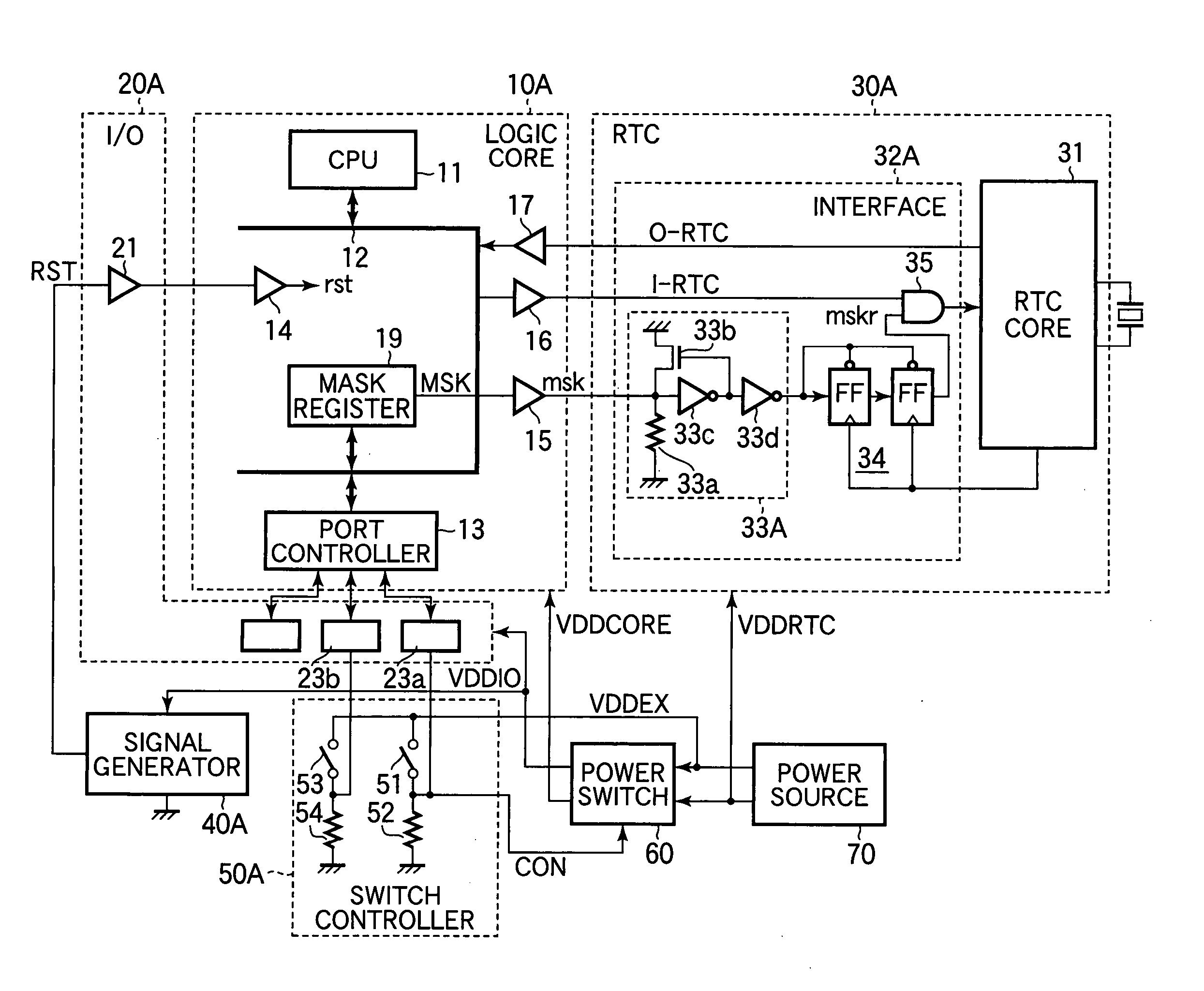
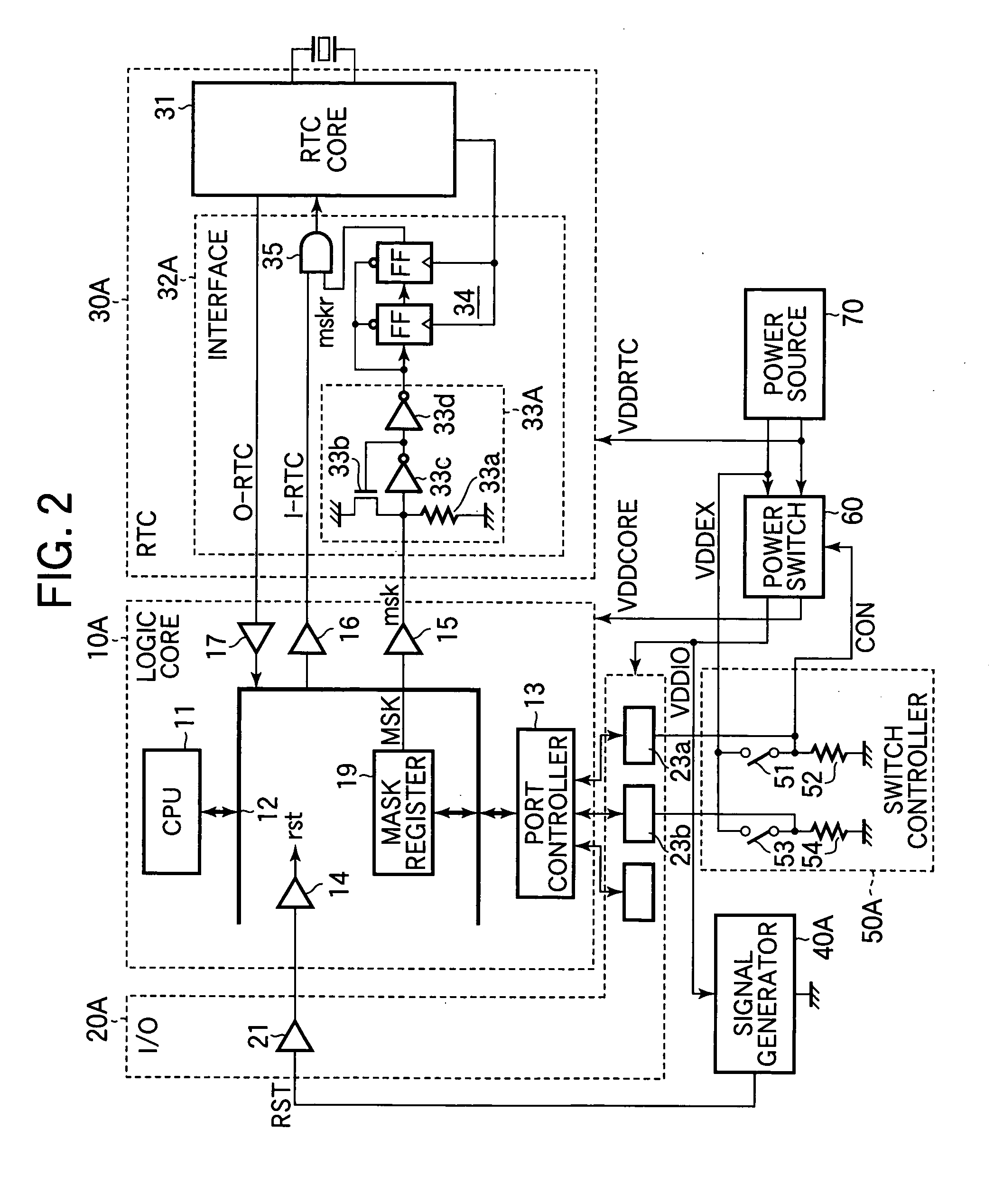
[0043] Referring to FIG. 2, the first embodiment is a semiconductor circuit comprising a large-scale integrated circuit, referred to below as an LSI chip, and external circuits connected to the LSI chip. The LSI chip includes a logic core 10A, an input-output section 20A, and a real-time clock counter or RTC 30A. The external circuits include a signal generator 40A, a switch controller 50A, a power switch 60, and a battery power source 70. The semiconductor circuit operates in a normal mode and a standby mode, referred to below as a battery backup mode.

[0044] The logic core 10A and input-output section 20A are disposed in a power-off area that receives power in the normal mode but not in the battery backup mode. The power supply voltage VDDCORE of the logic core 10A is substantially 1.5 V; the power supply voltage VDDIO of the input-output section 20A is substantially 3.3 V.

[0045] Like the logic core 10 in FIG. 1, the logic core 10A has a CPU 11, a system bus 12 c...

Example

Second Embodiment

[0075]FIG. 3 shows the RTC and its associated circuits in a second embodiment of the invention. The second embodiment differs from the first embodiment by replacing the logic core 10A and RTC 30A in the first embodiment in FIG. 2 with a modified logic core 10B and RTC 30B. The logic core 10B is modified by the addition of protective diodes 18 for the O-RTC signal line. The RTC 30B is modified by the addition of protective diodes 36, 37 for the mask (msk) and I-RTC signal lines, and an AND gate 38 that masks the O-RTC output signal when the synchronous mask signal (mskr) is low.

[0076] If there are multiple O-RTC signals, the second embodiment provides a separate AND gate 38 for each O-RTC signal line, each AND gate 38 receiving the synchronous mask signal (mskr) from the synchronizing circuit 34.

[0077] When the power of the power-off area is switched on, the logic core 10B and RTC 30B operate as described in the first embodiment, keeping the mask signals (MSK, msk...

Example

Third Embodiment

[0080]FIG. 4 shows the RTC and associated circuits in a third embodiment of the invention. The third embodiment differs from the second embodiment by replacing the RTC 30B in FIG. 3 with a modified RTC 30C in which the RTC core 31A has an additional state testing register 300. The state testing register 300 stores arbitrary data that can be read and written from the logic core 10B when the logic core 10B is powered and the mask is cleared. The RTC core 31A also includes a clock oscillator and further circuitry for generating time data as noted in the first embodiment.

[0081] The state testing register 300 is used as follows.

[0082] During power-up, after accessing the mask register and clearing the mask signal MSK as described in the first embodiment, the CPU in the logic core 10B writes a value other than zero in the state testing register 300, then reads the data in the state testing register 300. If the mask in the RTC 30C has been cleared (the synchronous mask s...


PUM


Abstract

A semiconductor circuit includes an integrated circuit having a backup area that is constantly powered and a power-off area that is powered off in a standby mode. A register in the power-off area stores a mask signal that is normally set to the high level but is changed to the low level before a transition to the standby mode. A latch circuit in the backup area latches the low level but not the high level of the mask signal. A masking circuit in the backup area masks input signals from the power-off area to the backup area while the latch circuit is in the latched state. Besides preventing erratic input to the backup area during normal-to-standby transitions, this arrangement prevents leakage of current from the backup area to the power-off area on the mask signal line in the standby mode.

Description

BACKGROUND OF THE INVENTION [0001] 1. Field of the Invention [0002] The present invention relates to power supply control in a semiconductor circuit. [0003] 2. Description of the Related Art [0004] As advances in semiconductor fabrication technology continue to reduce the sizes of transistors, the current that leaks through the transistors in the off-state continues to increase, causing large-scale integrated (LSI) circuits to draw significant amounts of current even in the standby state in which their input signals, output signals, and clock signals are all halted. This is a particularly serious problem for portable devices that operate on battery power; reducing the current consumption of these devices in the standby state has become a major issue. There are various ways to reduce the standby current consumed by an LSI circuit, the most effective of which is to use a switch to shut off its power supply. [0005] Shutting off the power supply of an entire LSI circuit chip presents no...

Claims


Application Information

Patent Timeline
IPC IPC(8): G06F1/26
CPCG06F1/3203E02D17/207E02D2250/003E02D2600/30
Inventor HASHIDATE, SHUICHI
Owner LAPIS SEMICON CO LTD
Why Eureka
Try Eureka