Semiconductor device and manufacturing method thereof

a technology of semiconductor devices and manufacturing methods, applied in semiconductor devices, semiconductor/solid-state device details, electrical apparatus, etc., can solve the problems of increasing manufacturing costs, difficult to uniformly form the above-mentioned inorganic insulation layer, and the shape of the package becomes larger

Inactive Publication Date: 2006-03-16
KK TOSHIBA
View PDF13 Cites 119 Cited by
  • Summary
  • Abstract
  • Description
  • Claims
  • Application Information

AI Technical Summary

Problems solved by technology

As in such stacked type multi-chip package, a package structure, in which the wiring bonding is applied to the connection between the semiconductor chip and the substrate, or between the plurality of semiconductor chips, causes an increase of manufacturing cost due to the cost necessary for the connecting processes and the man hours.
And in addition to a longer signal wiring length, it has a problem that the shape of package becomes larger.
However, it is difficult to uniformly form the above-mentioned inorganic insulation layer such as a SiO2 layer, a Si3N4 layer and the like on the inner surface of the through hole.
Particularly, it is difficult to form a thick film thereof.
Therefore, the inorganic insulation layer formed by applying a conventional semiconductor process has a main cause that an insulation reliability of the plug connecting the front and rear surfaces is decreased.
Further, when forming an inorganic insulation layer on an inner surface of the through hole, there is a problem that the filling of conductive material such as a metal and the like within the through hole is technically difficult.
However there is a problem that a mechanical strength of the semiconductor chip is decreased.

Method used


Image

  • Semiconductor device and manufacturing method thereof
  • Semiconductor device and manufacturing method thereof
  • Semiconductor device and manufacturing method thereof

Examples


first embodiment

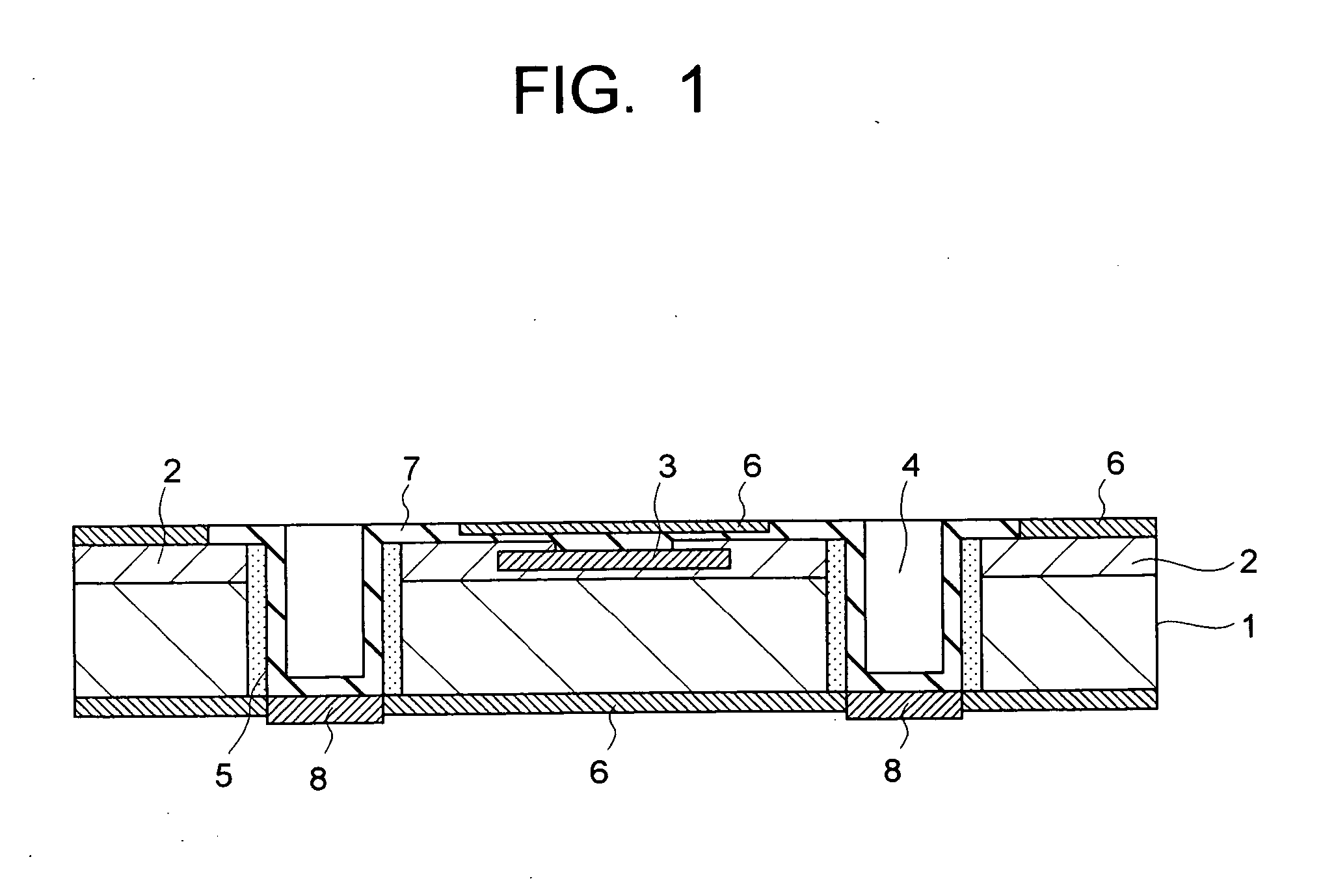
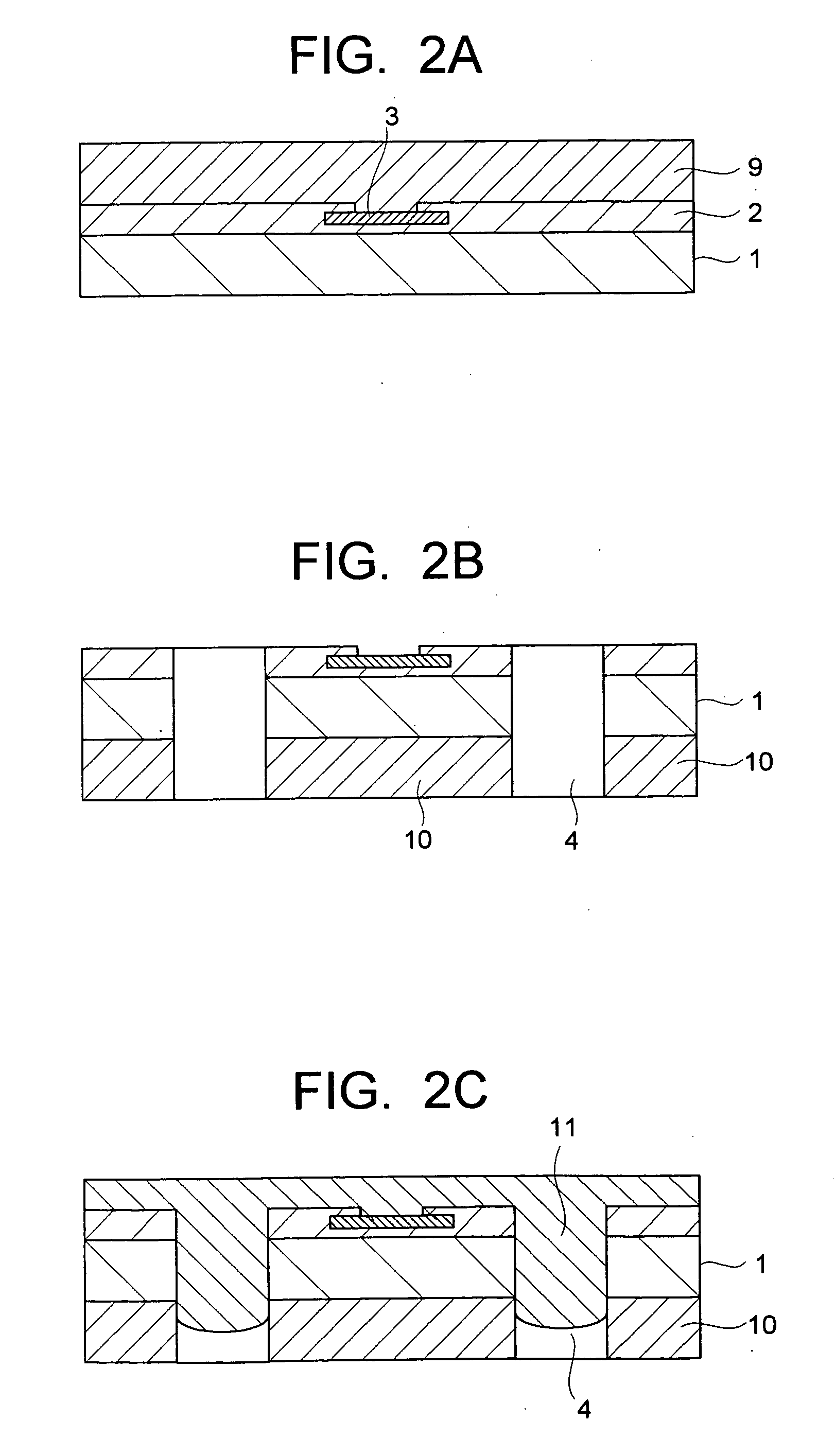
[0038]FIG. 1 is a cross sectional drawing showing a structure of a semiconductor device according to the present invention. Reference number 1 shows a semiconductor substrate such as a silicon substrate having a surface on which functional elements are integrated and formed. That is, at a surface side of the semiconductor substrate 1 which is an element region, an integrated element portion, a multiple layered wiring portion (silicon wiring layer) 2 connecting between respective elements, and the like are formed. Further, on a surface of the semiconductor substrate 1, an Al electrode (pad) 3 connecting to the multiple layered wiring portion being within the semiconductor substrate. The semiconductor substrate 1 has a through hole 4 passing through front and rear surfaces thereof. The through hole 4 is formed by irradiating a laser, and an inner surface (side wall surface) of the through hole 4 is composed of silicon having an amorphous structure.

[0039] And, on the inner surface of t...

second embodiment

[0057] as mentioned above, a semiconductor device suitable for a structure of stacking a plurality of semiconductor chips, and having a high reliability can be manufactured. And the manufacturing method is not necessary to use an expensive apparatus such as the RIE. In addition, since the method does not have much processes of mask exposure processes and developing processes, it is possible to obtain the semiconductor device with low cost.

[0058] Further, the forming of the through hole 4 to the semiconductor substrate 1 is carried out by the laser irradiating, and the inside wall of the through hole 4 is formed of silicon having an amorphous structure. Then the insulation resin 11 filled into the through hole 4 is strongly adhered with the inside wall of the through hole 4. In addition, the inside wall surface of the through hole 4 is completely covered with the insulation resin 11 which extends to the rear surface of the semiconductor substrate 1. Accordingly, the insulation betwe...

third embodiment

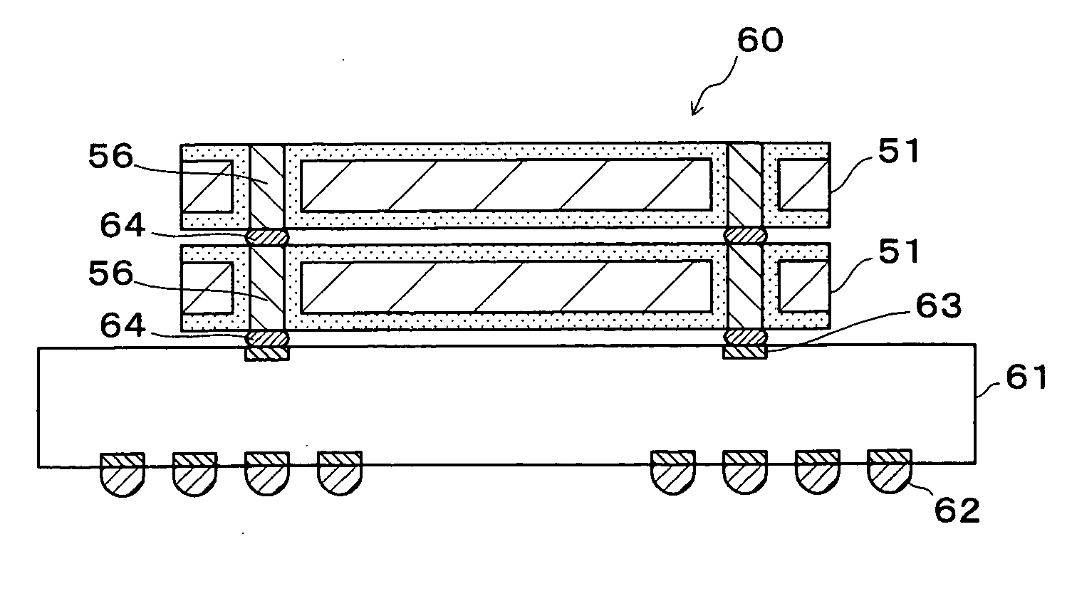
[0060] In the semiconductor device as shown in FIG. 3, in addition to the front surface of the semiconductor substrate 1, a wiring layer 24 is also formed on the rear surface thereof. In the rear surface of the semiconductor substrate 1, on the wiring layer 24 drawn out from the through via, a connecting electrode with other semiconductor device is formed.

[0061] For manufacturing the semiconductor device according to the third embodiment, similarly with the second embodiment, processes shown in FIG. 2A to FIG. 2J are carried out in turn, and then the glass supporting body 1 being on the rear surface is changed to stick on the front surface of the semiconductor substrate 1. And, on whole rear surface including the through hole 4 of the semiconductor substrate 1, a conductor metal layer (seeding layer metal) is formed by an electroless plating method, evaporation depositing method, or sputtering method.

[0062] Subsequently, a resist is formed on the conductor metal layer, and after e...


PUM


Abstract

A semiconductor device comprises a semiconductor substrate having an through hole, a first insulation resin layer formed on an inner surface of the through hole, a second insulation resin layer formed on at least one of front and rear surfaces of the semiconductor substrate, and a first conductor layer formed in the through hole to connect at least both front and rear surfaces of the semiconductor substrate and insulated from the inner surface of the through hole with the first insulation resin layer. A second conductor layer (wiring pattern) which is electrically connected to the first conductor layer in the through hole is further provided on the second insulation resin layer. The conductor layer formed in the through hole and constituting a connecting plug has a high insulation reliability. Therefore, a semiconductor device suitable for a multi-chip package and the like can be obtained. Further, since the forming ability of the conductor layer connecting the front and rear surfaces and the insulation layer is high, the manufacturing cost can be reduced.

Description

CROSS-REFERENCE TO RELATED APPLICATIONS [0001] This application is based upon and claims the benefit of the priority from the prior Japanese Patent Applications No. 2004-264729, No 2004-264731 and No. 2004-264732 filed on Sep. 10, 2004, respectively: the entire contents of which are incorporated herein by references. BACKGROUND [0002] 1. Field of the Invention [0003] This invention relates to a semiconductor device which can be applied as a multi-chip package having a plurality of semiconductor elements (semiconductor chips) and a manufacturing method thereof. [0004] 2. Description of the Related Art [0005] Recently, for realizing a miniaturization and a high density of a semiconductor device, a stacked type multi-chip package, in which a plurality of semiconductor elements (chips) are stacked and sealed in one package, is put to practical use. Generally, in the stacked type multi-chip package, respective electrode pads of a plurality pf semiconductor chips and an electrode portion ...

Claims


Application Information

Patent Timeline
Patent Type & Authority Applications(United States)
IPC IPC(8): H01L23/48
CPCH01L21/76898H01L23/481H01L25/0657H01L25/50H01L2224/16H01L2924/15311H01L2225/06541H01L2924/01046H01L2924/01078H01L2924/01079H01L2225/06513H01L2924/12044H01L2224/05569H01L2224/05008H01L2224/05022H01L2224/05001H01L2224/05147H01L2924/00014H01L2224/13025H01L24/19H01L24/05H01L24/03H01L2924/00H01L2224/05599H01L23/12
Inventor NUMATA, HIDEOEZAWA, HIROKAZUTAKUBO, CHIAKITAKAHASHI, KENJIAOKI, HIDEOHARADA, SUSUMUKANEKO, HISASHIIKENOUE, HIROSHIMATSUO, MIEOMURA, ICHIRO
Owner KK TOSHIBA
Why Eureka
Try Eureka