Apparatus for producing nitride semiconductor, method for producing nitride semiconductor, and semiconductor laser device obtained by the method

a technology of nitride semiconductor and semiconductor laser, which is applied in the direction of semiconductor laser, crystal growth process, polycrystalline material growth, etc., can solve the problems of preventing the uniform distribution of source gas concentration ratio, affecting the yield of nitride semiconductor lasers, and the use of conventional mocvd apparatus, etc., to achieve less varied optical characteristics and improve yield

Inactive Publication Date: 2006-03-16
SHARP KK +1
View PDF13 Cites 20 Cited by
  • Summary
  • Abstract
  • Description
  • Claims
  • Application Information

AI Technical Summary

Benefits of technology

[0039] The laser emission wavelength of the nitride semiconductor laser produced by using the apparatus for producing a nitride semiconductor according to the present invention has its variation restricted to 1 nm or less throughout the substrate plane. Further, the vari

Problems solved by technology

However, producing nitride semiconductor lasers of GaN, AlGaN, AlInGaN, etc., with the use of conventional MOCVD apparatuses are problematic in the following respects.
This prevents the uniformity of the concentration ratio distribution of the source gas of group III element and the concentration ratio distribution of the source gas of group V element over the plane of the substrate over which nitride semiconductors are crystal-grown to give a laminated structure of thin films.
As a result, the characteristics of resulting nitride semiconductor lasers are not uniform, presenting the problem of unsatisfactory yields.
Espec

Method used


Image

  • Apparatus for producing nitride semiconductor, method for producing nitride semiconductor, and semiconductor laser device obtained by the method
  • Apparatus for producing nitride semiconductor, method for producing nitride semiconductor, and semiconductor laser device obtained by the method
  • Apparatus for producing nitride semiconductor, method for producing nitride semiconductor, and semiconductor laser device obtained by the method

Examples


embodiment 1

[0075] MOCVD Apparatus

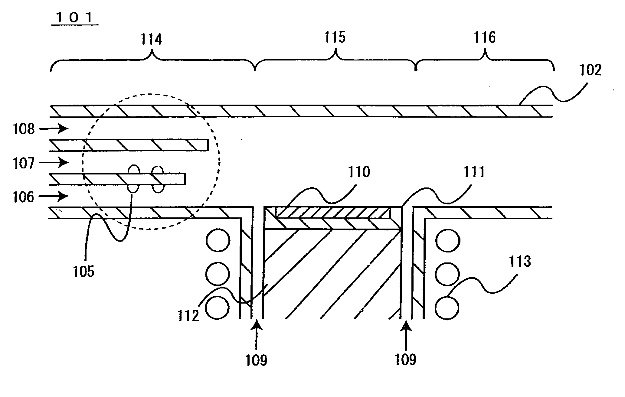
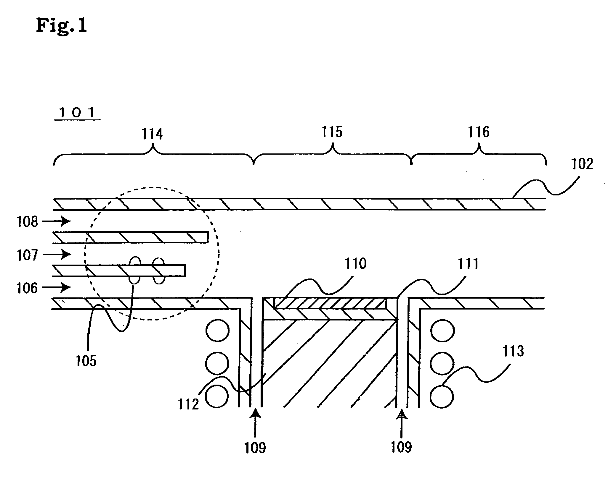
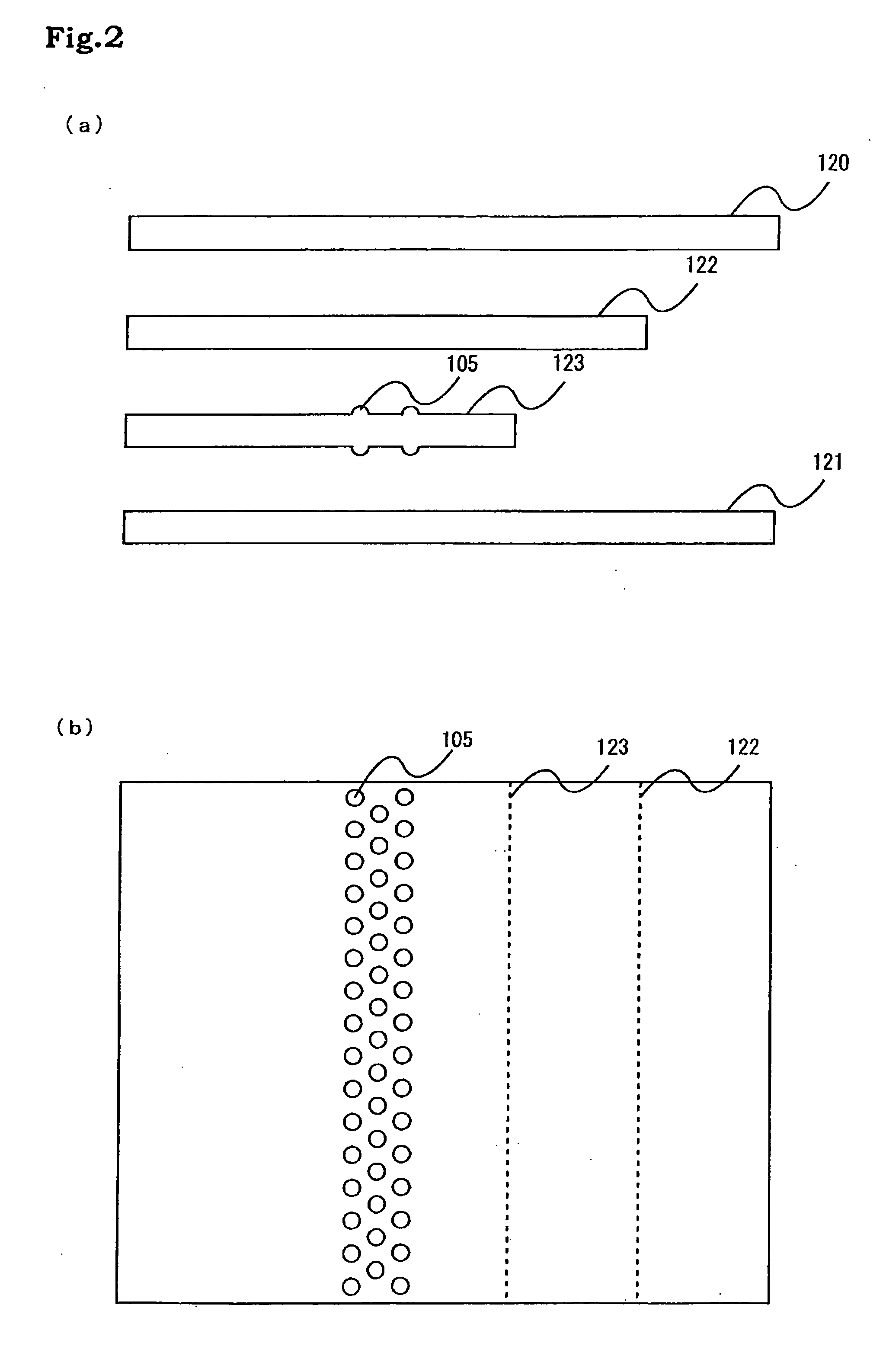
[0076] The MOCVD apparatus according to this embodiment of the present invention is as shown in FIG. 1 and has flow channel 102 of 100 mm wide in the inner diameter and of a height of 10 mm. A plurality of protrusions were provided on the partition between source NH3 gas line 106 and source MO gas line 107. The shape of protrusions 105 was hemispherical, the radius of the bottom surface thereof was 2 mm, and the height thereof was 2 mm. A plurality of protrusions 105 were provided 175 mm to 183 mm on the upstream side of the center of the substrate. Protrusions 105 were arranged periodically in such a pattern that the centers of three neighboring protrusions were 4 mm spaced from each other and make up the three apices of an equilateral triangle each side of which was 4 mm.

[0077] Epitaxial Growth of Nitride Semiconductor Layer

[0078] Next, a method for preparing a semiconductor laser device by forming nitride semiconductor layers over an n-type GaN substrate ...

embodiment 2

[0116] A nitride semiconductor laser was prepared in a similar manner to Embodiment 1 by using a MOCVD apparatus with protrusions provided on the inner wall of the upper surface of the flow channel, the inner wall of the lower surface of the flow channel, and the upper and lower surfaces of the partition between the protection gas line and III gas line. This nitride semiconductor laser also showed improvement in the in-plane uniformity of the laser emission wavelength and in the uniformity of Al composition of the first n-type AlGaN cladding layer throughout the substrate plane.

[0117] A nitride semiconductor laser was prepared in a similar manner to Embodiment 1 by using a MOCVD apparatus with the protrusions campanulate-shaped (trigonal pyramid-, quadrangular pyramid-, and cone-shaped) and column-shaped (triangular prism-, quadratic prism-, and cylinder-shaped) rather than hemisphere-shaped This nitride semiconductor laser also showed improvement in the in-plane uniformity of the ...

embodiment 3

[0120] Even when the size of the substrate was increased from 2 inches to 3 inches, the variation of laser emission wavelength of the nitride semiconductor laser produced by the apparatus for producing a nitride semiconductor according to the present invention was restricted to Inm or less throughout the substrate. Further, the variation of mixed crystal ratio of the AlGaN layer and the variation of thickness of the AlGaN layer throughout the substrate were restricted to several %. The MOCVD used here had a flow channel of 150 mm wide in the inner width and of a height of 12 mm. The shape of the protrusions was hemispherical, and the radius of the bottom surface was 2 mm and the height was 2 mm. Two or more protrusions were provided on the flow channel 220 mm to 236 mm on the upstream side of the center of the substrate. Also, two or more protrusions were arranged periodically in such a pattern that the centers of three neighboring protrusions were 4 mm spaced from each other and ma...


PUM

PropertyMeasurementUnit
Sizeaaaaaaaaaa
Semiconductor propertiesaaaaaaaaaa

Abstract

The present invention relates to an apparatus for producing a nitride semiconductor by crystal-growing the nitride semiconductor on a substrate by diffusing a gas containing a source gas of group III element and a source gas of group V element. The gas is diffused in parallel with the substrate and from upstream to downstream. The apparatus has the substrate housed in the apparatus and a flow channel for allowing the gas to flow in the flow channel. The apparatus also has a plurality of protrusions provided on an inner wall of the flow channel. A partition for causing the source gas of group III element and the source gas of group V element to be introduced separately into the flow channel is provided on the upstream portion of the flow channel and in a horizontal direction. The protrusions are formed on the upper and lower surfaces of the partition. With this structure, the source gas of group III element and the source gas of group V element are more uniformly mixed before the source gases are supplied.

Description

[0001] This non-provisional application claims priority under 35 U.S.C. §119(a) on Japanese Patent Application No. 2004-264162 filed in Japan on Sep. 10, 2004, the entire contents of which are hereby incorporated by reference. BACKGROUND OF THE INVENTION [0002] 1) Field of the Invention [0003] The present invention generally relates to an apparatus for producing a nitride semiconductor by crystal-growing the nitride semiconductor on a substrate by diffusing, from upstream to downstream, a gas that contains a source gas of group III element and a source gas of group V element. More specifically, the invention relates to an improved apparatus for producing a nitride semiconductor which makes the characteristics of the nitride semiconductor device uniform over the plane. The present invention also relates to an improved method for producing a nitride semiconductor laser device which makes the characteristics of the nitride semiconductor device uniform over the plane. The present invent...

Claims


Application Information

Patent Timeline
IPC IPC(8): C23C16/00H01L21/20
CPCB82Y20/00H01L21/0262C23C16/45504C23C16/45563C23C16/45574C30B25/14C30B29/403H01S5/0014H01S5/0202H01S5/34333H01S2304/04H01L21/02389H01L21/02458H01L21/02507H01L21/0254C23C16/303
Inventor ARAKI, MASAHIROYAMADA, EIJIYUASA, TAKAYUKITSUDA, YUHZOHAKUTSU, NAKAO
Owner SHARP KK
Why Eureka
Try Eureka