Method of stacking thin substrates by transfer bonding

Inactive Publication Date: 2006-03-16
AGENCY FOR SCI TECH & RES
View PDF11 Cites 241 Cited by
  • Summary
  • Abstract
  • Description
  • Claims
  • Application Information

AI Technical Summary

Benefits of technology

[0018] A second barrier layer and an insulative shield/passivation layer is deposited on the thinned first wafer and the layers are patterned to form contact windows and conductive links by conventional metallization and patterning process or by a damascene process, thereby making any interconnections between the circuits on the first and second wafers. Another layer of protective barrier and an insulative sh

Problems solved by technology

Although the concept of multilayered chips is old, the technology to produce them cost effectively was not available.
Such processes as SOI (Silicon On Insulator) and SOS (Silicon On Sapphire) as well a the bonding of discrete devices, such as MEMS (Micro-Electro-Mechanical-Systems) onto integrated circuit chips were well known but not cost or design effective.
In addition, these improvements have also allowed the formation of items, which were previously impossible because of processing incompatibilities.
The process is only capable of transferring deposit

Method used


Image

  • Method of stacking thin substrates by transfer bonding
  • Method of stacking thin substrates by transfer bonding
  • Method of stacking thin substrates by transfer bonding

Examples


first embodiment

[0029] In a first embodiment of this invention a stack of three interconnected integrated circuit layers is formed consisting of two thin silicon integrated circuit layers formed on a third integrated circuit layer, the later being formed on a conventional silicon wafer substrate. The embodiment illustrates not only the method forming and transfer bonding of multiple thin semiconductor device layers to create three dimensional integrated circuit chips but also the application of the method to interconnect devices on adjacent layers, non-adjacent layers, and multiple layers.

Formation of a First and Second Integrated Circuit layers

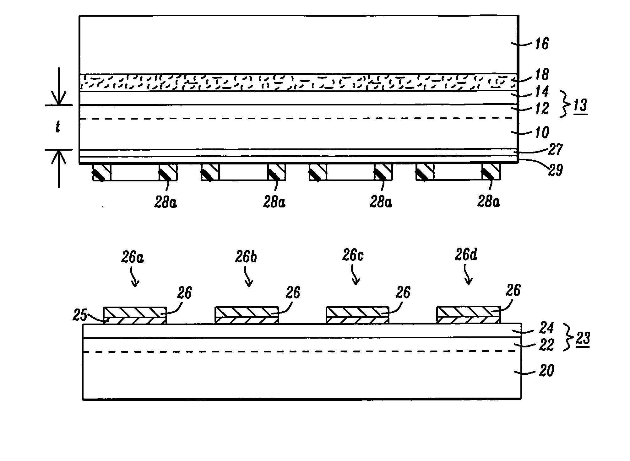
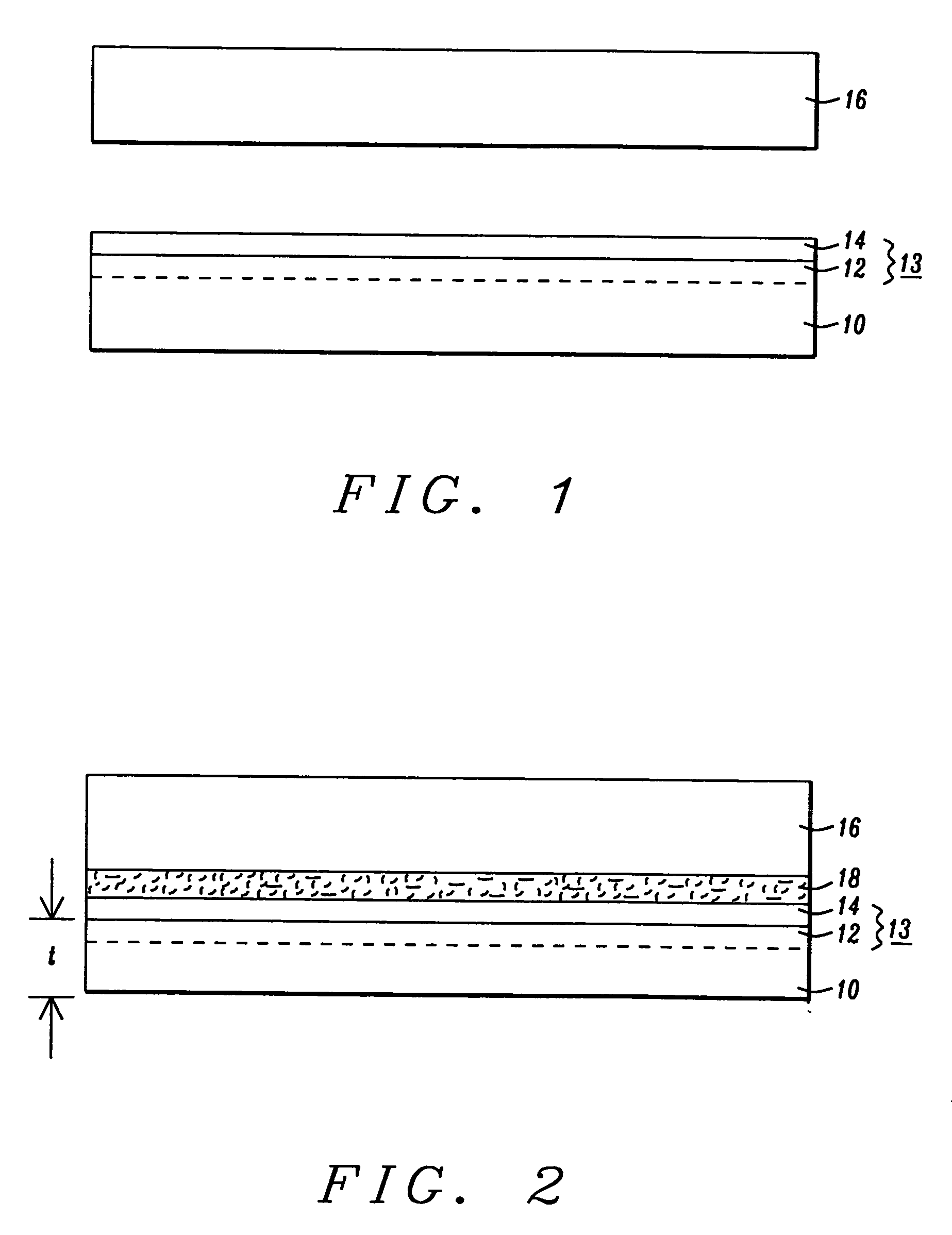
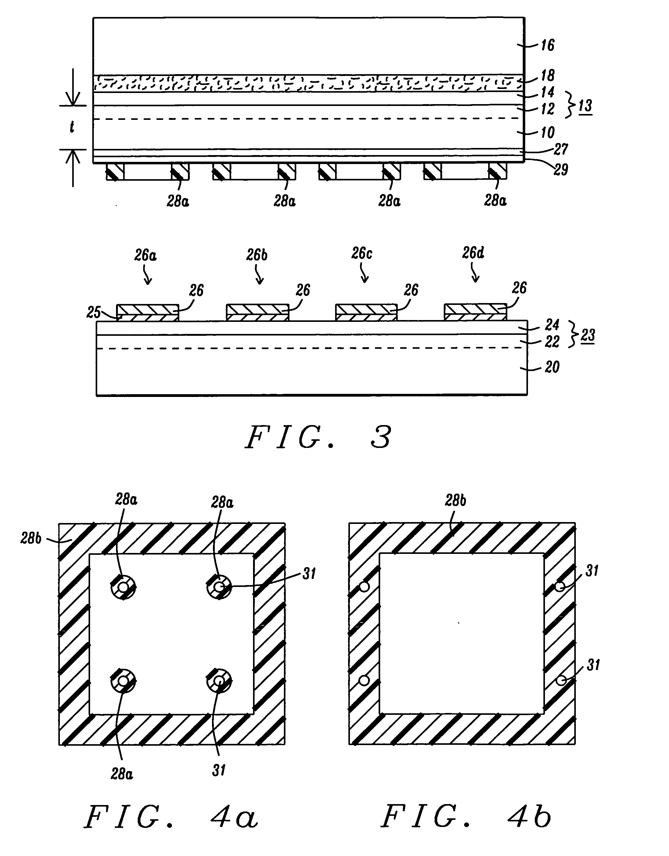
[0030] Referring to FIG. 1, a first silicon wafer 10 is prepared by conventional processing. Semiconductive devices are formed within the top surface 12 of the wafer 10 and a personalization layer 14 consisting of a plurality of wiring levels interleaved with ILD (interlevel dielectric) layers and interconnected with conductive contacts and vias are forme...

second embodiment

[0052] In a second embodiment of this invention a stack of three interconnected integrated circuit layers is formed consisting of two thin silicon integrated circuit layers formed on a third integrated circuit layer, the later being formed on a conventional silicon wafer substrate. The second embodiment is an alternative to the first embodiment supra and is identical to the first embodiment except that the blanket resin adhesive layer which is used to bind the thinned integrated circuit layers is not patterned after the layer is deposited. Instead, the entire adhesive layer is used to bond the integrated circuit layers together. Later, when the deep pass through openings are formed in the uppermost stacked integrated circuit layer the anisotropic etching process is extended to remove the resin layer at the base of the opening. The second embodiment is identical to the first embodiment up to the point where the handler mounted first wafer 10 has been thinned as illustrated in FIG. 2....

third embodiment

[0064] In a third embodiment of this invention a stack of two interconnected integrated circuit layers is formed by first bonding two silicon wafers and then thinning one of the two wafers, thereby eliminating the need for temporary bonding to a separate handler. The first wafer is a blank unprocessed wafer and the second wafer has an integrated circuit layer comprising a masterslice layer consisting of active and passive silicon devices and a personalization layer comprising wiring circuitry terminating in bond pads on a top passivation layer. In addition, the embodiment also illustrates how a multilayer integrated circuit package can be prepared for dicing during stack formation.

[0065] Referring to FIG. 17 a first un-processed blank silicon wafer 210, is provided. An insulative layer 227, preferably silicon oxide between about 500 and 1000 nm thick, and a barrier / passivation layer 229, preferably silicon nitride, between about 50 and 100 nm thick are sequentially deposited on the...


PUM


Abstract

This invention describes a method of stacking, bonding, and electrically interconnecting a plurality of thin integrated circuit wafers to form an interconnected stack of integrated circuit layers. The first integrated circuit layer is formed by conventional processing on a silicon wafer to the stage where bond pads are patterned on a wiring layer interconnecting the subjacent semiconductive devices. The remaining integrated circuit layers are formed by first processing a standard wafer to form integrated circuit devices and wiring levels up to but not including bond pads. Each of these wafers is mounted onto a handler wafer by its upper face with a sacrificial bonding agent. The wafer is thinned, permanently fastened to the top surface of the first base wafer by a non-conductive adhesive applied to the thinned under face, and dismounted from the handler. Vertical openings are etched through the thinned layer to the bond pads on the subjacent wafer. Robust conductive pass-through plugs with integrated upper bond pads are formed in the openings. Additional thinned integrated circuit layers may be prepared, thinned, cemented onto the stack. Wiring interconnections can be made between any two or more layers. The process is unique in that it can be used to further stack and interconnect any number of thinned wafer layers to form a three dimensional integrated circuits, including MEMS devices. This approach provides a low temperature wafer bonding method using an adhesive which results in process simplicity and cost effectiveness by eliminating an additional masking and patterning process for under bump metal thereby enabling standard wafers to be integrated into a 3D stack with existing wire bonded wafers.

Description

[0001] This application claims priority to U.S. Provisional Patent Application Ser. No. 60 / 609,131, filed on Sep. 10, 2004, which is herein incorporated by reference in its entirety.BACKGROUND OF THE INVENTION [0002] (1) Field of the Invention [0003] The invention relates to processes for the manufacture of integrated circuits and more particularly to the area of forming three-dimensional integrated circuits by wafer stacking. [0004] (2) Background of the Invention and Description of Previous Art [0005] In the apparent never ending quest towards further miniaturization and increasing circuit density of solid state integrated circuits, the technology has been forced to develop new packaging approaches, other than discrete single surface silicon chips. One such approach involves packaging integrated circuits using multiple chips layered and interconnected one upon the other. Although the concept of multilayered chips is old, the technology to produce them cost effectively was not avai...

Claims


Application Information

Patent Timeline
IPC IPC(8): H01L21/4763H01L21/44H01L21/30
CPCH01L21/76898H01L23/481H01L2924/07802H01L2224/0401H01L2924/10253H01L2924/0002H01L2924/01019H01L2924/01006H01L2224/9202H01L24/12H01L24/16H01L25/0657H01L25/50H01L2224/04042H01L2224/0557H01L2224/13009H01L2224/13099H01L2225/06513H01L2225/06541H01L2924/01005H01L2924/01007H01L2924/01013H01L2924/01014H01L2924/01022H01L2924/01028H01L2924/01029H01L2924/01049H01L2924/0105H01L2924/01073H01L2924/01074H01L2924/01078H01L2924/01079H01L2924/04941H01L2924/04953H01L2924/05042H01L2924/09701H01L2924/14H01L2924/3025H01L24/05H01L2924/00H01L2224/05552
Inventor NAGARAJAN, RANGANATHANSANKARAPILLAI, CHIRAYARIKATHUVEEDU PREMACHANDRAN
Owner AGENCY FOR SCI TECH & RES
Why Eureka
Try Eureka