Loop-back method for measuring the interface timing of semiconductor memory devices using the normal mode memory

Inactive Publication Date: 2006-03-16
INFINEON TECH AG
View PDF9 Cites 13 Cited by
  • Summary
  • Abstract
  • Description
  • Claims
  • Application Information

AI Technical Summary

Benefits of technology

[0039] The provision of the parity bits thus makes it possible to obtain an

Problems solved by technology

In particular, the size of the test pattern can only

Method used


Image

  • Loop-back method for measuring the interface timing of semiconductor memory devices using the normal mode memory
  • Loop-back method for measuring the interface timing of semiconductor memory devices using the normal mode memory
  • Loop-back method for measuring the interface timing of semiconductor memory devices using the normal mode memory

Examples


first embodiment

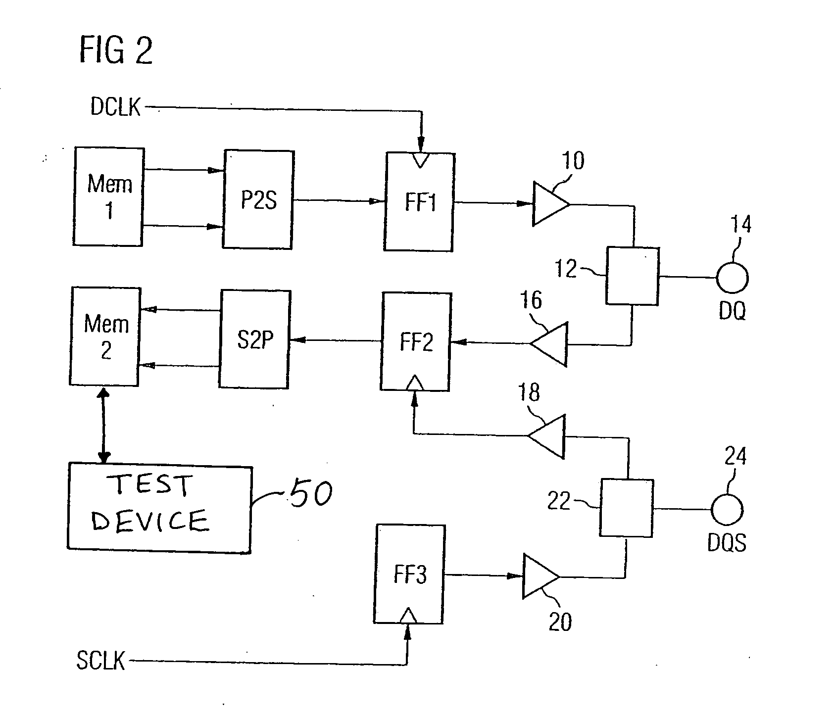
[0091]FIG. 2 shows a similar view to FIG. 1. Elements of the semiconductor memory device which are the same as in the first embodiment are designated by the same reference symbols, and a detailed description thereof is dispensed with.

[0092] The semiconductor memory device in accordance with the second embodiment generally has the same structure as the semiconductor memory device in accordance with the first embodiment, the difference being that the comparison device 26 is not provided. In the semiconductor memory device shown, the output of the second flip-flop FF2 is signal-connected to a second memory area Mem 2 via a serial-to-parallel conversion device S2P.

[0093] The functioning of the semiconductor memory device during normal operation is the same as that of the semiconductor memory device in accordance with the first embodiment.

[0094] In test operation, the output signal of the second flip-flop FF2 is not compared with the test input data, as in the first embodiment. Rather,...

third embodiment

[0096] A third preferred embodiment of the present invention will now be described with reference to FIG. 3. FIG. 3 is a schematic view of a semiconductor memory device in accordance with a

[0097] The embodiment shown in FIG. 3 corresponds to that embodiment shown in FIG. 2 with the difference that an external loop is formed in the test mode. In this case, a first data contact 30 is signal-connected to a second data contact 32 via an external load resistor RL. The first data contact 30 is signal-connected to a first data pad 34, and the second data contact 32 is signal-connected to a second data pad 36. In a similar manner, two data clock contacts 38 and 40 are signal-connected to one another via an external load resistor RL during the test mode.

second embodiment

[0098] In the test mode, an external loop is formed by the output driver 10, which is signal-connected to the first data pad 34, the first data contact 30, the second data contact 32, the second data pad 36 and the input driver 16, which is signal-connected to the second data pad 36. In this case, the output drivers 10 and input drivers 16 are in each case switched such that the output driver 10 associated with a first data contact enables a signal transmission, and the input driver 16 of the associated data contact 32 in the pair-wise arrangement of two data contacts enables a signal transmission. The respective other output drivers 10 and input drivers 16 are switched such that signal transmission is not made possible. A similar arrangement is produced for the data clock signals DQS. The operation of the semiconductor memory device in the test mode is the same as that in accordance with the second embodiment, and a detailed description thereof is dispensed with.

[0099] Further embo...


PUM


Abstract

The invention relates to a method for testing a semiconductor memory device, the semiconductor memory device being able to be operated in a normal operating mode and a test mode. The method for testing includes communicating test input data to be used for a test to the semiconductor memory device; storing the test input data in memory cells of a memory area of the semiconductor memory device; and reading out the stored test input data from the memory cells for carrying out a test in order to obtain test output data, the memory area in which the test input data are stored in the test mode being used for storing data in the normal operating mode. In addition, the invention relates to a semiconductor memory device and a system for testing a semiconductor memory device.

Description

CROSS-REFERENCE TO RELATED APPLICATIONS [0001] This application claims foreign priority benefits under 35 U.S.C. §119 to co-pending German patent application number DE 10 2004 043051.9, filed 6 Sep. 2004. This related patent application is herein incorporated by reference in its entirety. BACKGROUND OF THE INVENTION [0002] 1. Field of the Invention [0003] The present invention relates to a method and a system for testing a semiconductor memory device, and to a semiconductor memory device. [0004] 2. Description of the Related Art [0005] Methods for testing semiconductor memory devices, in particular, methods for testing the interface timing, are known such that a test pattern is communicated to and stored in the semiconductor memory device. In this case, a particular memory area is provided for storing the test pattern. In addition, a multiplexer is provided in the semiconductor memory device, which makes it possible to change over between the memory area used in a normal operating m...

Claims


Application Information

Patent Timeline
IPC IPC(8): G11C29/00
CPCG11C29/022G11C29/50012G11C29/50
Inventor SPIRKL, WOLFGANG
Owner INFINEON TECH AG
Why Eureka
Try Eureka