

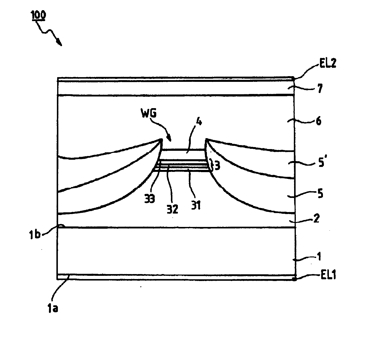
Semiconductor optical device on an indium phosphide substrate for long operating wavelengths
a technology of indium phosphide and optical devices, applied in semiconductor lasers, lasers, radiation controlled devices, etc., can solve the problem of not providing useful wavelengths, and achieve the effect of increasing the thermal performance of lasers
- Summary
- Abstract
- Description
- Claims
- Application Information
AI Technical Summary
Benefits of technology
Problems solved by technology
Method used
Image

Examples
example 1
[0061] The quantum-well layer is of In0.4Ga0.6As0.995N0.005 with thickness chosen to be 14 nm for example. The operating wavelength is 1.55 μm. The quantum-well layer has a tensile stress of about 1%.
[0062] In the example the barrier layers are of Al0.31In0.69As and of thickness equal to about 10 nm.
example 2
[0063] The quantum-well layer is of In0.38Ga0.62As0.99N0.01 with thickness chosen to be 10 nm for example. The operating wavelength is 1.55 μm. The quantum-well layer has a tensile stress of about 1.25%.
[0064] In the example the barrier layers are of Al0.31In0.69As and of thickness equal to about 10 nm.
example 3
[0065] The quantum-well layer is of In0.4Ga0.6As0.99N0.01 with thickness chosen to be 14 nm for example. The operating wavelength is 1.60 μm. The quantum-well layer has a tensile stress of about 1.1%.
[0066] In the example the barrier layers are of Al0.3In0.69As and of thickness equal to about 10 nm.
PUM
 Abstract
Description
Claims
Application Information