Nitride semiconductor light emitting device having electrostatic discharge(ESD) protection capacity

a technology of nitride semiconductor and light emitting diodes, which is applied in the direction of semiconductor devices, basic electric elements, electrical apparatus, etc., can solve the problems of weak static electricity resistance of damage to nitride semiconductor light emitting diodes, etc., and achieve the effect of minimizing the increase of their overall size and number

Active Publication Date: 2006-03-23
SAMSUNG ELECTRONICS CO LTD
View PDF8 Cites 108 Cited by
  • Summary
  • Abstract
  • Description
  • Claims
  • Application Information

AI Technical Summary

Benefits of technology

[0011] Therefore, the present invention has been made in view of the above problems, and it is an object of the invention to provide a nitride semiconductor light emitting device for simultaneously implementing a light emitting diod

Problems solved by technology

The nitride semiconductor light emitting diode has a disadvantage in that it has very weak resistance to static electricity as compared to other compound semiconductors such as GaP or GaAlAs.
For example, the nitride semiconductor light emitting diode may be damaged by a forward constant voltage of several hundreds of volts (e.g., 100V), and may also be damaged by a reverse constant voltage of several tens of volts (e.g., 30V).
Nitride semiconductor light emitting diodes are very vulnerable to the above-mentioned constant-voltages and may be damaged thereby when they are handled.
The above-mentioned electrostatic discharge (ESD) protection LED 10 implements each of the LED unit A and the diode B on the substrate 11, suc

Method used


Image

  • Nitride semiconductor light emitting device having electrostatic discharge(ESD) protection capacity
  • Nitride semiconductor light emitting device having electrostatic discharge(ESD) protection capacity
  • Nitride semiconductor light emitting device having electrostatic discharge(ESD) protection capacity

Examples


Embodiment Construction

[0025] Now, preferred embodiments of the present invention will be described in detail with reference to the annexed drawings. In the drawings, the same or similar elements are denoted by the same reference numerals even though they are depicted in different drawings. In the following description, a detailed description of known functions and configurations incorporated herein will be omitted when it may make the subject matter of the present invention rather unclear.

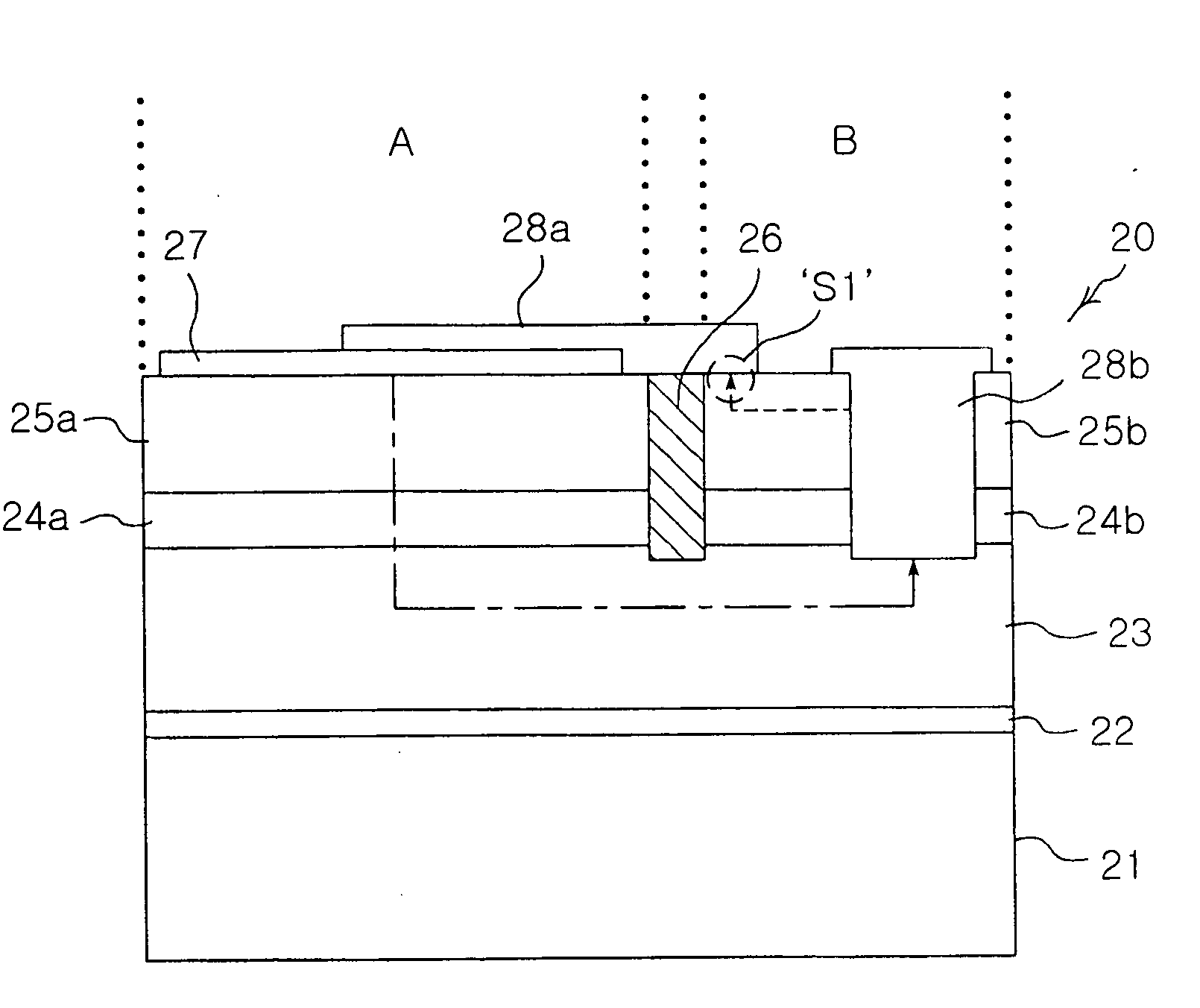
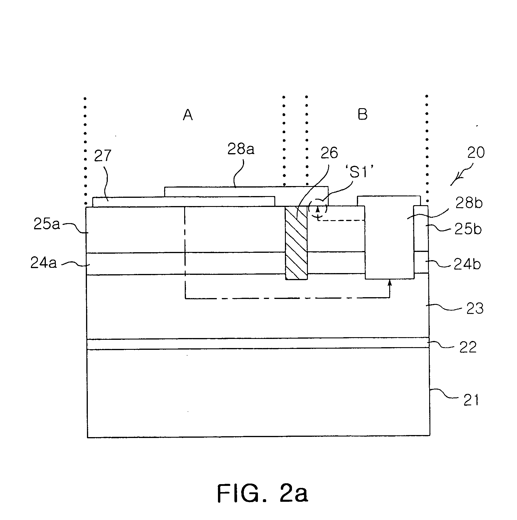
[0026]FIG. 2a is a cross-sectional view illustrating a nitride semiconductor light emitting device in accordance with a preferred embodiment of the present invention. FIG. 2b is a plan view illustrating the nitride semiconductor light emitting device of FIG. 2a. Referring to FIGS. 2a-2b, the nitride semiconductor light emitting device 20 in accordance with a preferred embodiment of the present invention forms a buffer layer 22 on a substrate 21, forms an n-type nitride semiconductor layer 23 on the buffer layer 22, for...


PUM


Abstract

A nitride semiconductor light emitting device including a light emitting diode and a diode formed on a single substrate, in which the light emitting diode and the diode use a common electrode. According to the present invention, an active layer and a p-type nitride semiconductor layer are each divided into a first region and a second region by an insulative isolation layer, and an ohmic contact layer is formed on the p-type nitride semiconductor layer contained in the first region. A p-type electrode is formed on the ohmic contact layer and is extended to the p-type nitride semiconductor layer contained in the second region. An n-type electrode is formed on the p-type nitride semiconductor layer contained in the second region, passes through the p-type nitride semiconductor layer and the active layer contained in the second region, and is connected to the first n-type nitride semiconductor layer.

Description

RELATED APPLICATIONS [0001] The present application is based on, and claims priority from, Korean Application Number 2004-74656, filed Sep. 17, 2004, the disclosure of which is incorporated by reference herein in its entirety. BACKGROUND OF THE INVENTION [0002] 1. Field of the Invention [0003] The present invention relates to a nitride semiconductor light emitting device, and more particularly to a nitride semiconductor light emitting device including a light emitting diode and a diode that are formed on a single substrate, which allows the light emitting diode and the diode to use a common electrode, so that it prevents the light emitting diode from being damaged by static electricity, and reduces the size of an overall device and the number of necessary electrodes. [0004] 2. Description of the Related Art [0005] In recent times, nitride semiconductors have been introduced, which use a nitride such as GaN, and have excellent physical and chemical characteristics so that they are in...

Claims


Application Information

Patent Timeline
IPC IPC(8): H01L29/22H01L33/32H01L33/40H01L33/62
CPCH01L27/15H01L2224/16225H01L2224/05573H01L2224/05568H01L2924/00014H01L2224/0554H01L2224/05599H01L2224/0555H01L2224/0556
Inventor LEE, KYU HANKIM, HYUN KYUNGKIM, JE WONKIM, DONG JOON
Owner SAMSUNG ELECTRONICS CO LTD
Why Eureka
Try Eureka