Semiconductor device packaged into chip size and manufacturing method thereof

a technology of semiconductor devices and chips, which is applied in the direction of semiconductor devices, semiconductor/solid-state device details, electrical apparatus, etc., can solve the problems of increasing and affecting the sealing effect of sealing materials, so as to reduce the cost of sealing materials and the manufacturing method of such devices

Inactive Publication Date: 2006-03-23
TERAMIKROS INC
View PDF8 Cites 80 Cited by
  • Summary
  • Abstract
  • Description
  • Claims
  • Application Information

AI Technical Summary

Benefits of technology

[0007] It is an object of the present invention to provide a semiconductor devi

Problems solved by technology

Since an organic material such as an epoxy-based resin or a polyimide-based resin which is a material of the second and third sealing films contains impurities such as an Na ion, a K ion, a Ca ion and Cl ion, a high concentration of the impurities can be a factor which provokes corrosion of the wiring or the columnar electrode or short circuit between t

Method used


Image

  • Semiconductor device packaged into chip size and manufacturing method thereof
  • Semiconductor device packaged into chip size and manufacturing method thereof
  • Semiconductor device packaged into chip size and manufacturing method thereof

Examples


Embodiment Construction

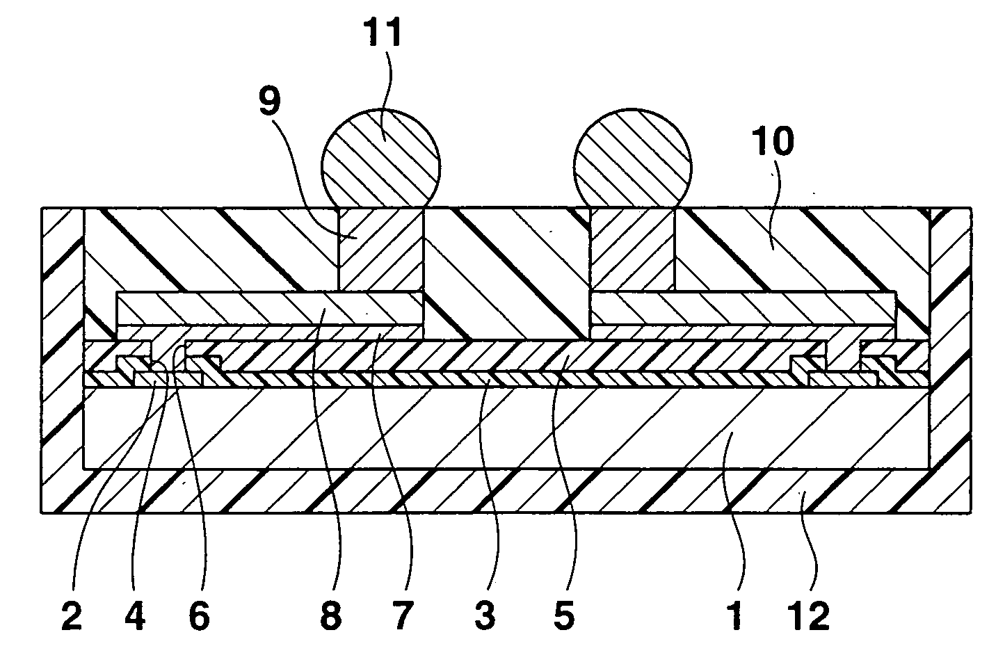
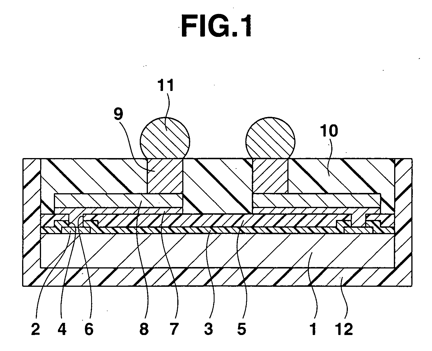
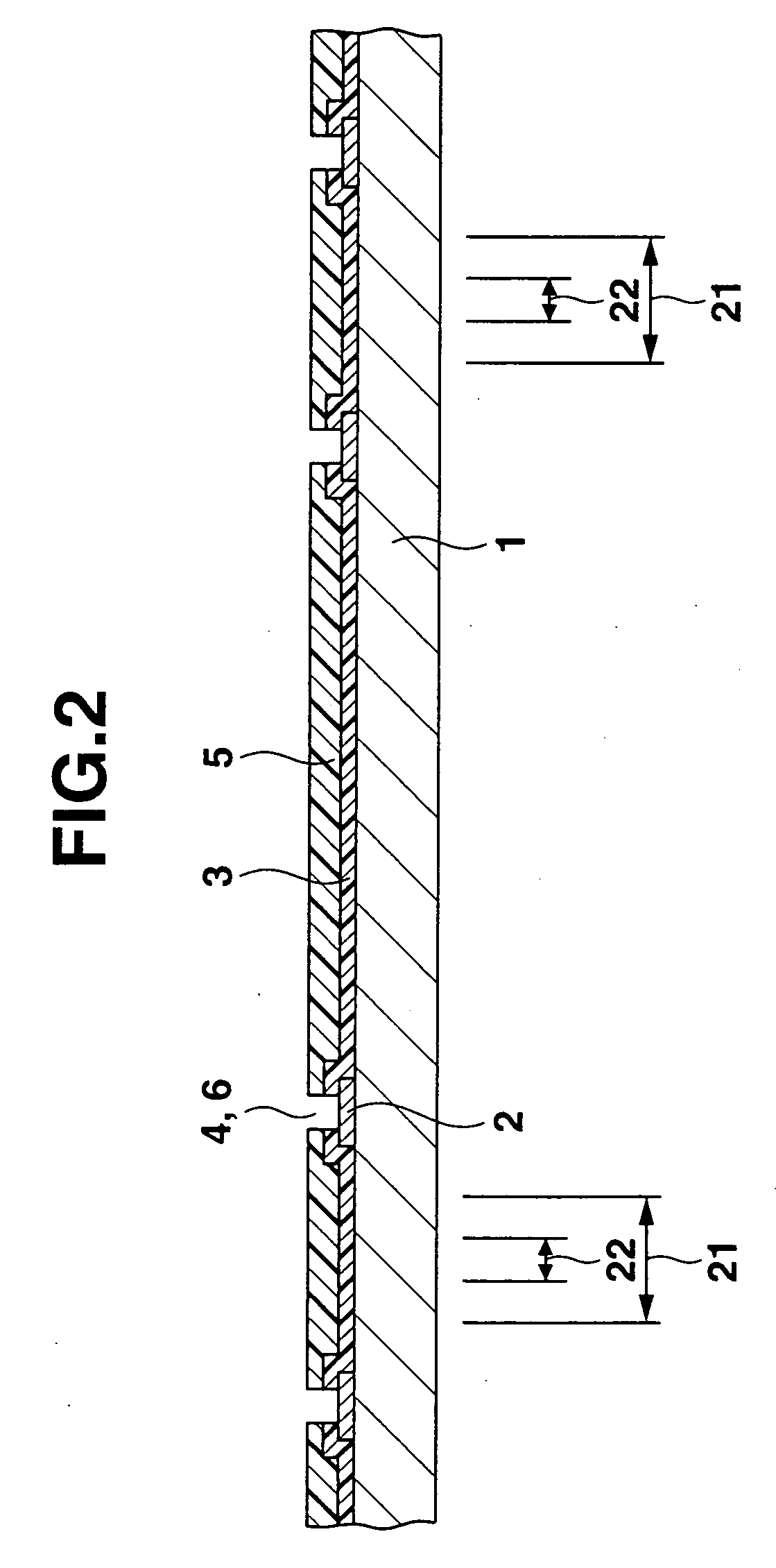
[0038]FIG. 1 is a cross-sectional view of a semiconductor device according to an embodiment of the present invention. This semiconductor device is generally called a CSP (chip size package), and provided with a silicon substrate (a semiconductor substrate) 1. An integrated circuit (not shown) having a predetermined function is provided on an upper surface of the silicon substrate 1, and a plurality of connection pads 2 formed of, e.g., an aluminum-based metal are electrically connected with the integrated circuit at an upper surface peripheral portion.

[0039] An insulating film 3 formed of, e.g., silicon oxide or silicon nitride is provided on the upper surface of the silicon substrate 1 excluding a central portion of each connection pad 2, and the central portion of the connection pad 2 is exposed through an opening portion 4 provided to the insulating film 3. A protection film (an insulating film) 5 formed of, e.g., an epoxy-based resin or a polyimide-based resin is provided on an...


PUM


Abstract

A semiconductor device includes a semiconductor substrate having an integrated circuit and at least one connection pad, and at least one external connection electrode electrically connected with the connection pad. A first sealing material is provided on the semiconductor substrate around the external connection electrode, each impurity concentration of an Na ion, a K ion, a Ca ion and Cl ion contained in the first sealing material being not greater than 10 ppm. A second sealing material is provided on at least one of a lower surface and a peripheral side surface of the semiconductor substrate, a total impurity concentration of an Na ion, a K ion, a Ca ion and a Cl ion contained in the second sealing material being not smaller than 100 ppm.

Description

CROSS-REFERENCE TO RELATED APPLICATIONS [0001] This application is based upon and claims the benefit of priority from prior Japanese Patent Applications No. 2004-270646, filed Sep. 17, 2004; and No. 2005-100737, filed Mar. 31, 2005, the entire contents of both of which are incorporated herein by reference. BACKGROUND OF THE INVENTION [0002] 1. Field of the Invention [0003] The present invention relates to a semiconductor device packaged into a chip size and a manufacturing method thereof. [0004] 2. Description of the Related Art [0005] Some of semiconductor devices having a conventional chip size have a configuration in which a lower surface of a semiconductor substrate having on an upper surface thereof an integrated circuit and a plurality of connection pads connected with the integrated circuit is covered with a first sealing film, the upper surface and peripheral side surfaces of the semiconductor substrates are covered with a second sealing film, a wiring is provided on an uppe...

Claims


Application Information

Patent Timeline
IPC IPC(8): H01L23/48
CPCH01L21/568H01L21/6835H01L24/13H01L21/78H01L23/3114H01L23/3135H01L24/10H01L24/96H01L24/97H01L2221/68331H01L2221/6834H01L2221/68363H01L2224/13099H01L2224/16H01L2924/01011H01L2924/01013H01L2924/0102H01L2924/01022H01L2924/01029H01L2924/01078H01L2924/14H01L2924/01005H01L2924/01006H01L2924/01019H01L2924/01033H01L2924/014H01L2924/00H01L2224/13H01L2224/05569H01L2224/05008H01L2224/05022H01L2224/05001H01L2224/05124H01L2224/05147H01L2224/05166H01L2224/05647H01L2924/3511H01L2224/04105H01L24/05H01L24/03H01L2924/0001H01L2224/02377H01L24/02H01L2924/00014H01L2224/02H01L23/10
Inventor WAKABAYASHI, TAKESHIMIHARA, ICHIRO
Owner TERAMIKROS INC
Why Eureka
Try Eureka