Process and apparatus for producing a substrate having a coating resin layer
a technology of coating resin and substrate, which is applied in the direction of coatings, pretreated surfaces, semiconductor devices, etc., can solve the problems of increasing the power generation the disadvantages of resin sealing methods, and the unavoidable cost of solar cells, so as to reduce the maintenance frequency of the apparatus, simplify the constitution of the apparatus, and improve the operation efficiency of the apparatus
- Summary
- Abstract
- Description
- Claims
- Application Information
AI Technical Summary
Benefits of technology
Problems solved by technology
Method used
Image
Examples
example 1
1. Preparation of Photovoltaic Element:
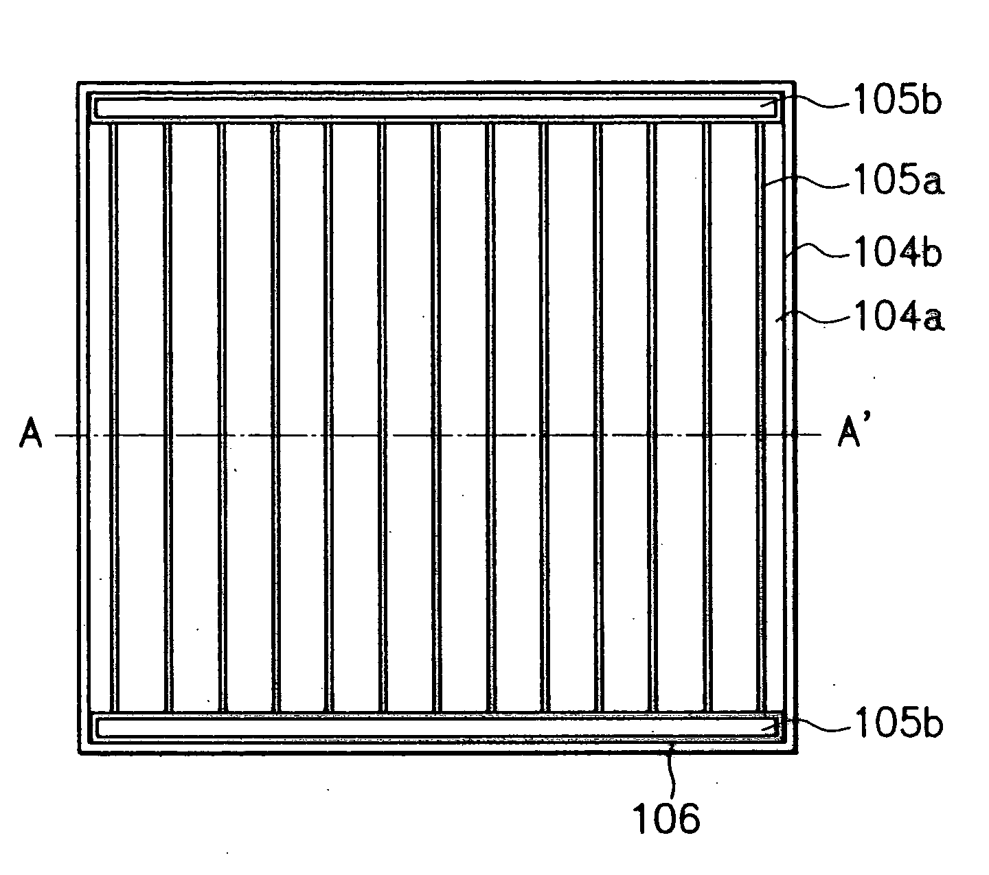
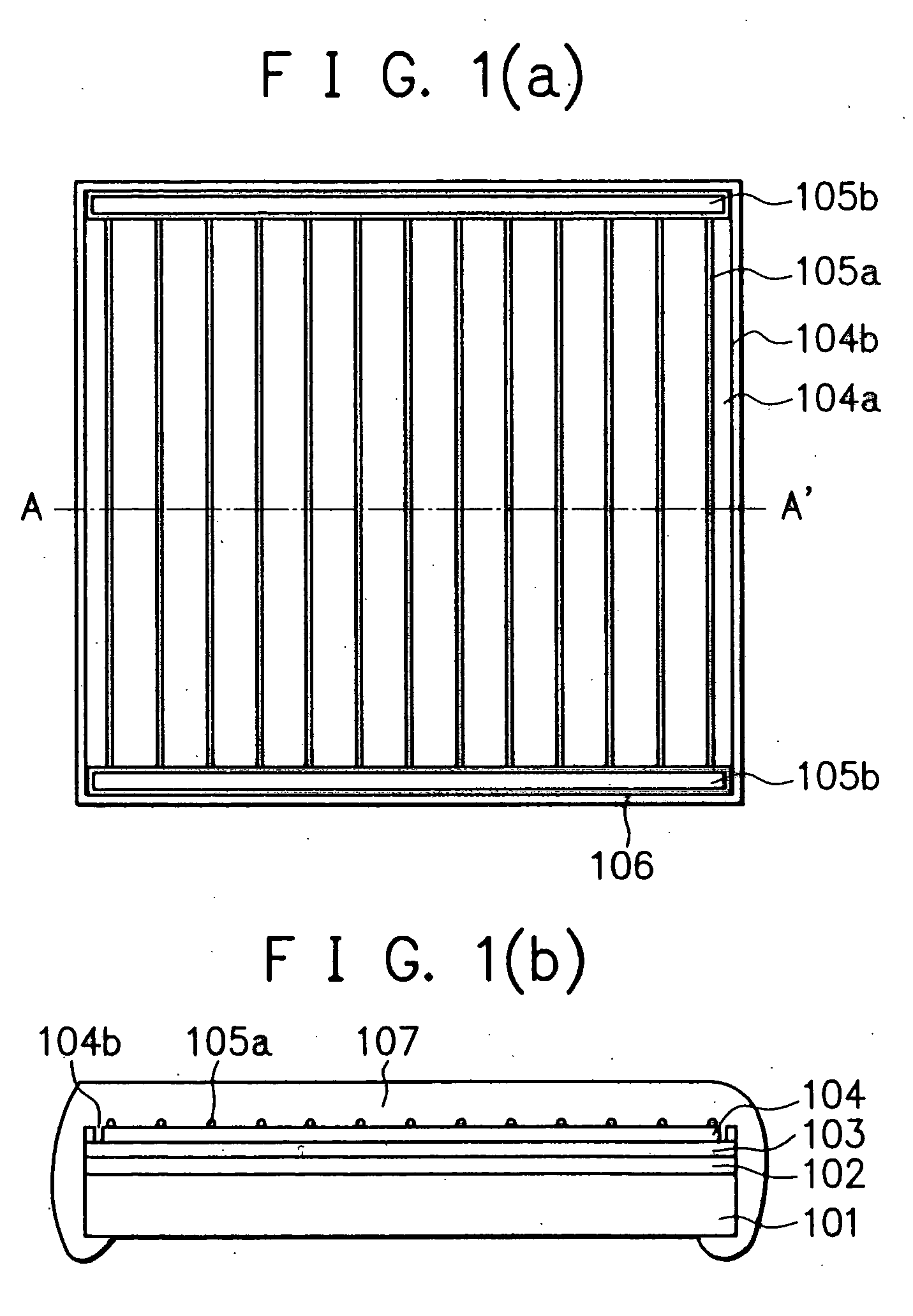
[0095] An amorphous silicon (a-Si) photovoltaic element having such configuration as shown in FIGS. 1(a) and 1(b) with no resin layer 107 was prepared in the following manner.
[0096] There was provided a well-cleaned stainless web substrate having a thickness of 150 μm and a width of 355 mm as the substrate 101. On the web substrate, there was formed a two-layered back reflecting layer 102 comprising a 5000 Å thick Al film / a 5000 Å thick ZnO film by means of the conventional roll-to-roll sputtering process.
[0097] On the back reflecting layer 102 thus formed, there was formed a tandem type photoelectric conversion semiconductor layer as the semiconductor active layer 103 comprising a 150 Å thick n-type amorphous silicon layer / a 4000 Å thick i-type amorphous silicon layer / a 100 Å thick p-type microcrystalline silicon layer / a 100 Å thick n-type amorphous silicon layer / a 800 Å thick i-type amorphous silicon layer / a 100 Å thick p-type microcrysta...
example 2
[0126] The procedures of Example 1 were repeated, except that a curtain coater was used as the spouting means and the spouting width of the resin layer precursor to get down on the surface of the photovoltaic element was made to be 300 mm, to obtain three photovoltaic elements having a resin-sealed structure.
[0127] The resultant three photovoltaic elements were evaluated in the same manner as in Example 1. The evaluated results are shown in Table 1.
PUM
| Property | Measurement | Unit |
|---|---|---|
| viscosity | aaaaa | aaaaa |
| total light transmittance | aaaaa | aaaaa |
| total light transmittance | aaaaa | aaaaa |
Abstract
Description
Claims
Application Information


