
Circuit-level memory and combinational block modeling

a combinational block and circuit-level memory technology, applied in the field of memory modeling, can solve the problems of inefficiency and waste of design resources, memory models from one eda tool vendor can typically only be used with simulation or verification engines from the same vendor, and prior art memory models suffer from two major disadvantages

Inactive Publication Date: 2006-03-23
AVERANT
View PDF15 Cites 0 Cited by
  • Summary
  • Abstract
  • Description
  • Claims
  • Application Information

AI Technical Summary

Problems solved by technology

However, prior art memory models suffered from two major disadvantages.
The resulting memory model was inefficient and wasted valuable design resources.
Second, memory models from one EDA tools vendor can typically only be used with simulation or verification engines from the same vendor.
This lack of interoperability greatly limits the utility of prior art memory models.

Method used


Image

  • Circuit-level memory and combinational block modeling
  • Circuit-level memory and combinational block modeling
  • Circuit-level memory and combinational block modeling

Examples


Embodiment Construction

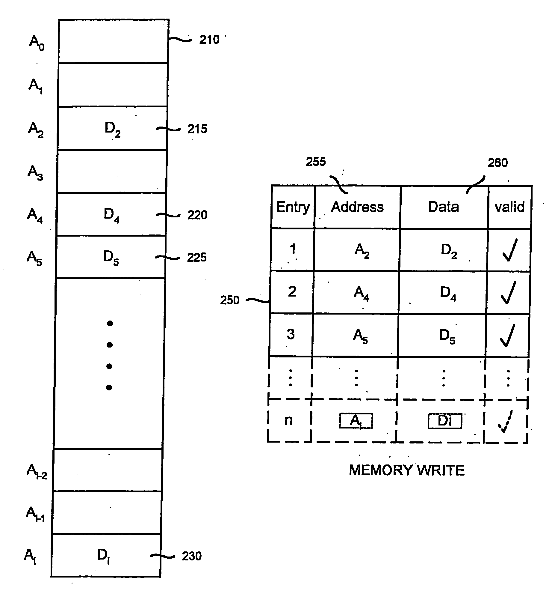
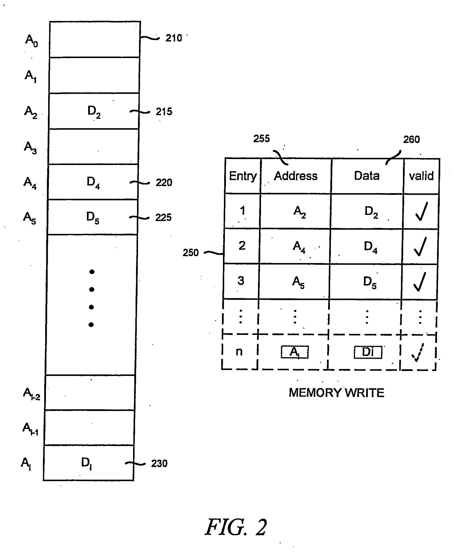
[0022]FIG. 2 illustrates a memory model that can be implemented as lookup table 250, for use in modeling a physical memory 210 of an electronic circuit design. While physical memory 210 contains “i” locations, data has been written to only four of those locations. In physical memory 210, for example, the electronic circuit design has written a plurality of write data bits represented by D2 to write address A2. A plurality of write data bits represented by D4 have been written to write address A4. A plurality of write data bits represented by D5 have been written to write address A5. A plurality of write data bits represented by Di have been written to write address Ai. Rather than modeling all “i” locations of physical memory 210, the present invention models only those locations of physical memory 210 that have been accessed by the electronic circuit design. Lookup table 250 is created to perform this task. Lookup table 250 comprises an address field 255, a data field 260, and a va...


PUM


Abstract

A method and apparatus for creating a memory model for use in modeling a physical memory of an electronic circuit design. Memory write operations to the physical memory and memory read operations are modeled in a lookup table. The number of entries in the lookup table is limited by an upper bound representing a total number of memory operations that can occur over a given number of clock cycles.

Description

[0001] This application is a continuation application of U.S. patent application Ser. No. 09 / 586,191, entitled “CIRCUIT-LEVEL MEMORY AND COMBINATIONAL BLOCK MODELING,” filed Jun. 2, 2000, incorporated herein by reference in its entirety.BACKGROUND OF THE INVENTION [0002] 1. Field of the Invention [0003] The present invention relates to electronic design automation (EDA) systems. More particularly, the present invention relates to memory modeling for use with EDA tools. [0004] 2. Description of the Related Art [0005] The design process for integrated circuits typically involves multiple transformations of a design from an initial idea to a functional, manufacturable product. A chip architect or designer begins with a design idea and then generates a corresponding behavioral definition of the design. The behavioral design results in a flow chart or a flow graph using which the designer can design the system data path and the registers and logic units necessary for implementation of th...

Claims


Application Information

Patent Timeline
Patent Type & Authority Applications(United States)
IPC IPC(8): G06F17/50G06G7/62
CPCG06F17/5022G06F30/33
Inventor ISLES, ADRIAN J.
Owner AVERANT
Learn More