Radiation image detector

Inactive Publication Date: 2006-03-30
FUJIFILM HLDG CORP +1
View PDF2 Cites 24 Cited by
  • Summary
  • Abstract
  • Description
  • Claims
  • Application Information

AI Technical Summary

Benefits of technology

[0012] In view of the circumstances described above, it is an object of the present invention to provide a TFT readout system radiation image detector capable of satisfactorily eliminating the noise signals generated by the parasitic capacitances with a simple and inexpensive circuit configuration.
[0026] According to the radiation image detector of the present invention, multitudes of dummy signal lines are provided, each being installed adjacent to each of the corresponding charge signal lines of the radiation image recording medium. This allows the capacitance value of each of the parasitic capacitors formed in the vicinity of the intersection between each of the gate control signal lines and each of the charge signal lines, and that of the corresponding parasitic capacitor formed in the vicinity of the intersection between each of the gate control signal lines and each of the dummy signal lines to be substantially equal to each other. In addition, each of the dummy signals flowed out to each of the dummy signal lines is subtracted from each of the corresponding charge signals flowed out to each of the charge signal lines, so that the noise signals generated by the parasitic capacitors formed in the vicinity of the respective intersections between the gate control signal lines and charge signal lines may be eliminated satisfactorily.

Problems solved by technology

Accordingly, the noise signals and noise compensation signals may differ in magnitude and the noise may not be eliminated properly, resulting in the residual noise being included in the charge signals.
Further, it requires a separate gate driver for outputting the reverse polarity signal to the noise compensation signal lines, causing the circuit to be more complicated and resulting in higher costs.

Method used


Image

  • Radiation image detector
  • Radiation image detector
  • Radiation image detector

Examples


Embodiment Construction

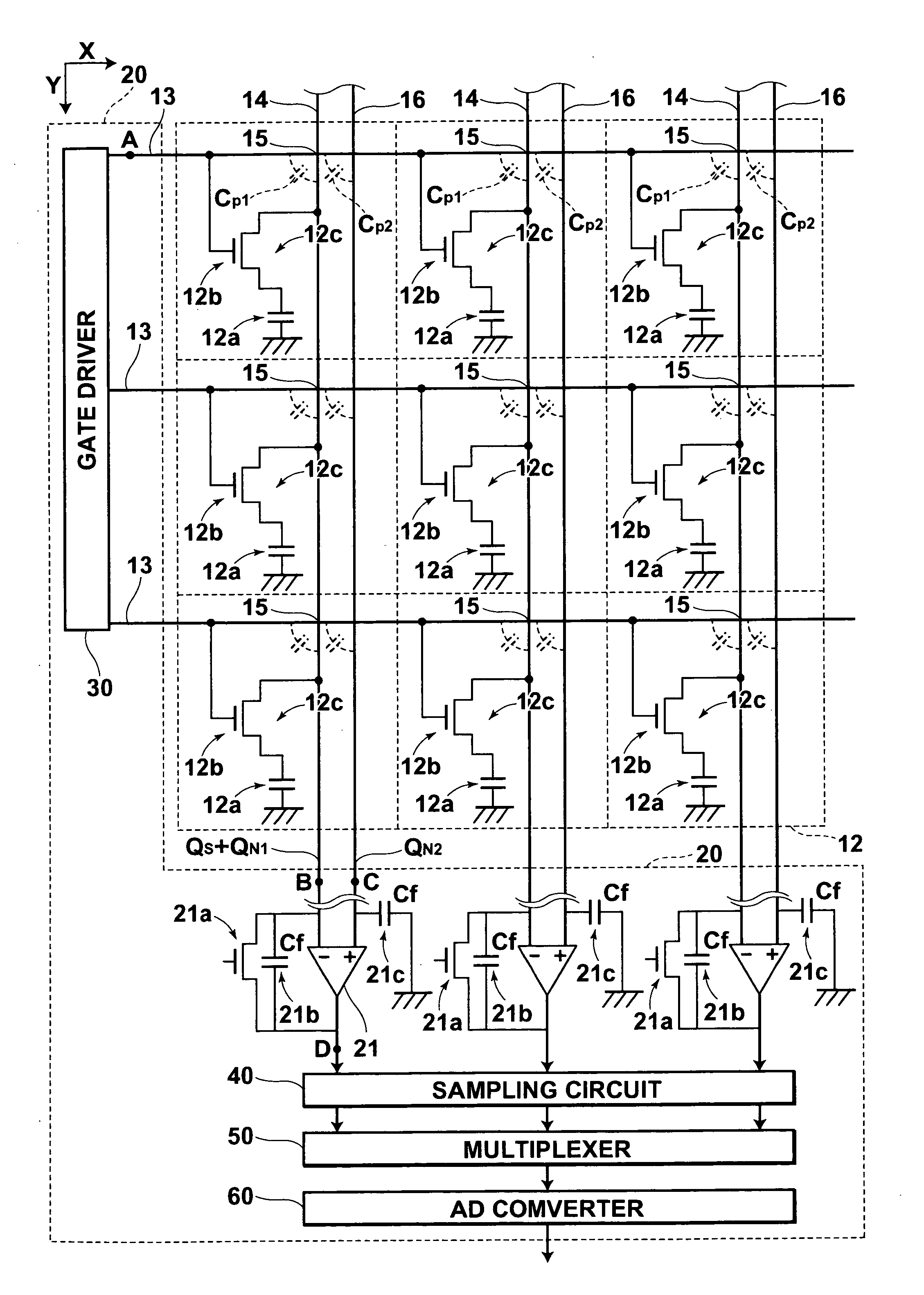
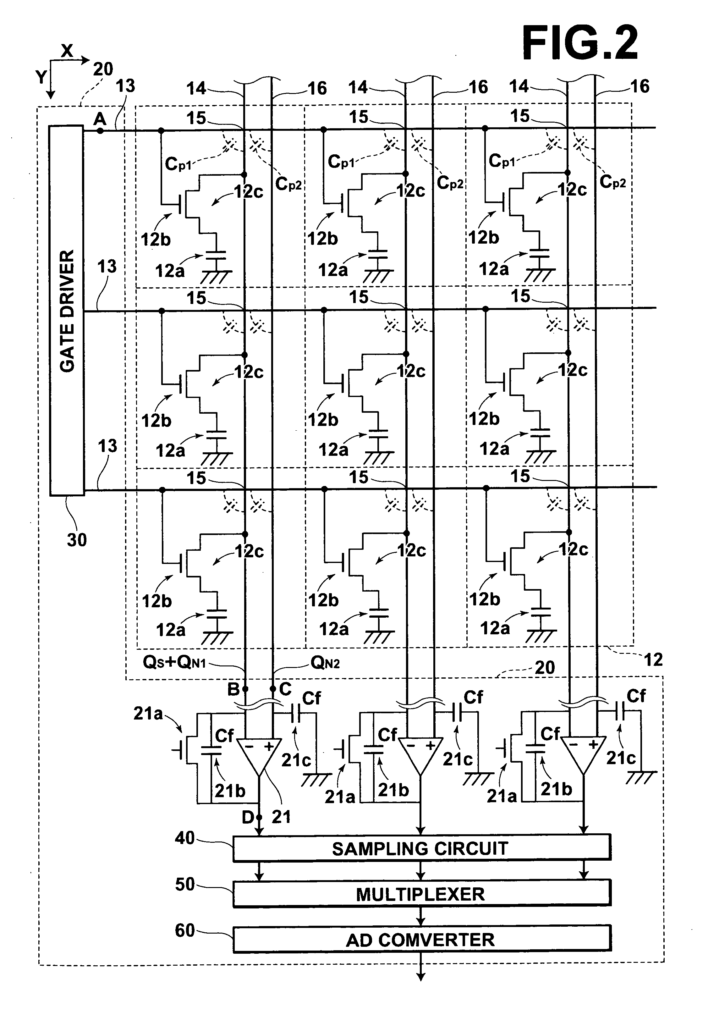
[0032] Hereinafter, an embodiment of the radiation image detector of the present invention will be described with reference to the accompanying drawings.

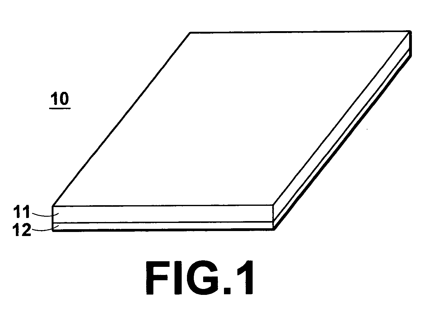
[0033] The radiation image detector according to the present embodiment includes a radiation image recording medium 10 having a charge generating layer 11 for generating charges by receiving radiation, and a charge detecting layer 12 for storing the charges generated in the charge generating layer 11 as shown in FIG. 1; and a detecting section 20, which will be described later, for detecting charge signals flowed out from the radiation image recording medium 10.

[0034] The charge generating layer 11 may be made of any material as long as it is capable of generating charges when exposed to radiation. Preferably, however, it is made of, for example, a-Se or the like which has high quantum efficiency and a less amount of dark current. Alternatively, the charge generating layer 11 may be a two-layer composite of a phosphor layer that e...


PUM


Abstract

A TFT readout system radiation image detector capable of satisfactorily removing noise signals generated by the parasitic capacitors formed in the vicinity of the respective intersections between gate control signal lines and charge signal lines with a simple and inexpensive circuit configuration. The detector includes charge detecting elements for storing charges generated by receiving radiation; gate control signal lines through which a gate control signal flows to control the switching element of each charge detecting element; charge signal lines to which charge signals stored in the storage sections flow out; and dummy signal lines, each being installed adjacent to each of the corresponding charge signal lines. The dummy signal flowed out to each dummy signal line is subtracted from the signal flowed out to each charge signal line when the gate signal is flowed through the gate control signal line by the differential amplifier.

Description

BACKGROUND OF THE INVENTION [0001] 1. Field of the Invention [0002] The present invention relates to a radiation image detector in which charges of a radiation image are generated and stored by receiving radiation carrying the radiation image, and the charges stored in the detector are detected as image signals. [0003] 2. Description of the Related Art [0004] Various types of radiation image detectors are proposed and put into practical use in the medical and other industrial fields. In such a detector, a radiation image of a subject is recorded by receiving radiation transmitted through the subject, and the image recorded on the detector is detected by reading out the image signals in accordance with the image recorded on the detector. [0005] Some of the radiation image detectors use, for example, a semiconductor material that generates charges when exposed to radiation, and some of them use a so-called TFT readout system. [0006] One such TFT readout system radiation image detector...

Claims


Application Information

Patent Timeline
IPC IPC(8): G01T1/24G01T1/17G01T1/20H01L27/14H01L27/144H04N5/32H04N5/335H04N5/357H04N5/369H04N5/376H04N5/378
CPCG01T1/2928H04N5/378H04N5/357H04N5/32H04N25/60H04N25/75
Inventor YAMAGUCHI, AKIRA
Owner FUJIFILM HLDG CORP
Why Eureka
Try Eureka