Integrated fuses for OLED lighting device

a technology of integrated fuses and lighting devices, which is applied in the direction of discharge tubes/lamp details, organic semiconductor devices, discharge tubes luminescnet screens, etc., can solve the problems of cumbersome manufacturing of lighting devices with external contacts for each strip, increased complexity of driver circuitry, and increased complexity of connection components, so as to reduce current flow across the fuse material and increase the resistivity of the fuse material

Active Publication Date: 2006-03-30
OSRAM OLED
View PDF8 Cites 50 Cited by
  • Summary
  • Abstract
  • Description
  • Claims
  • Application Information

AI Technical Summary

Benefits of technology

[0007] An embodiment of a method to operate a fault-tolerant electroluminescent lighting device is also described. The lighting device includes an electrode that is patterned into a plurality of electrode strips and a particular one of the electrode strips includes a gap that separates the particular electrode strip into a first electrode segment and a second electrode segment. A fuse material at least partially covers the gap such that the first electrode segment is electrically connected to the second electrode segment. The method to operate the device includes driving a current across the fuse material, and if the current driven across the fuse material is high, then the resistivity of the fuse material is increased so that current flow across the fuse material is decreased.

Problems solved by technology

Shorts may occur in any of the layers forming the element and may be caused by, for example, substrate imperfections or asperities, anode layer irregularities, non-uniformity of the one or more organic layers, and airborne particles introduced in the element structure during handling.
While a pixel failure due to a short in an OLED display renders the display useless, a failure of a strip in the OLED lighting device may be acceptable as long as the resulting output luminance is not significantly deteriorated.
Manufacturing the lighting device with the external contacts for each strip is cumbersome.
Also, external fuses also increase the complexity of the driver circuitry and the complexity of the connection components (e.g., the contact pad and the flex connector).

Method used


Image

  • Integrated fuses for OLED lighting device
  • Integrated fuses for OLED lighting device
  • Integrated fuses for OLED lighting device

Examples


first embodiment

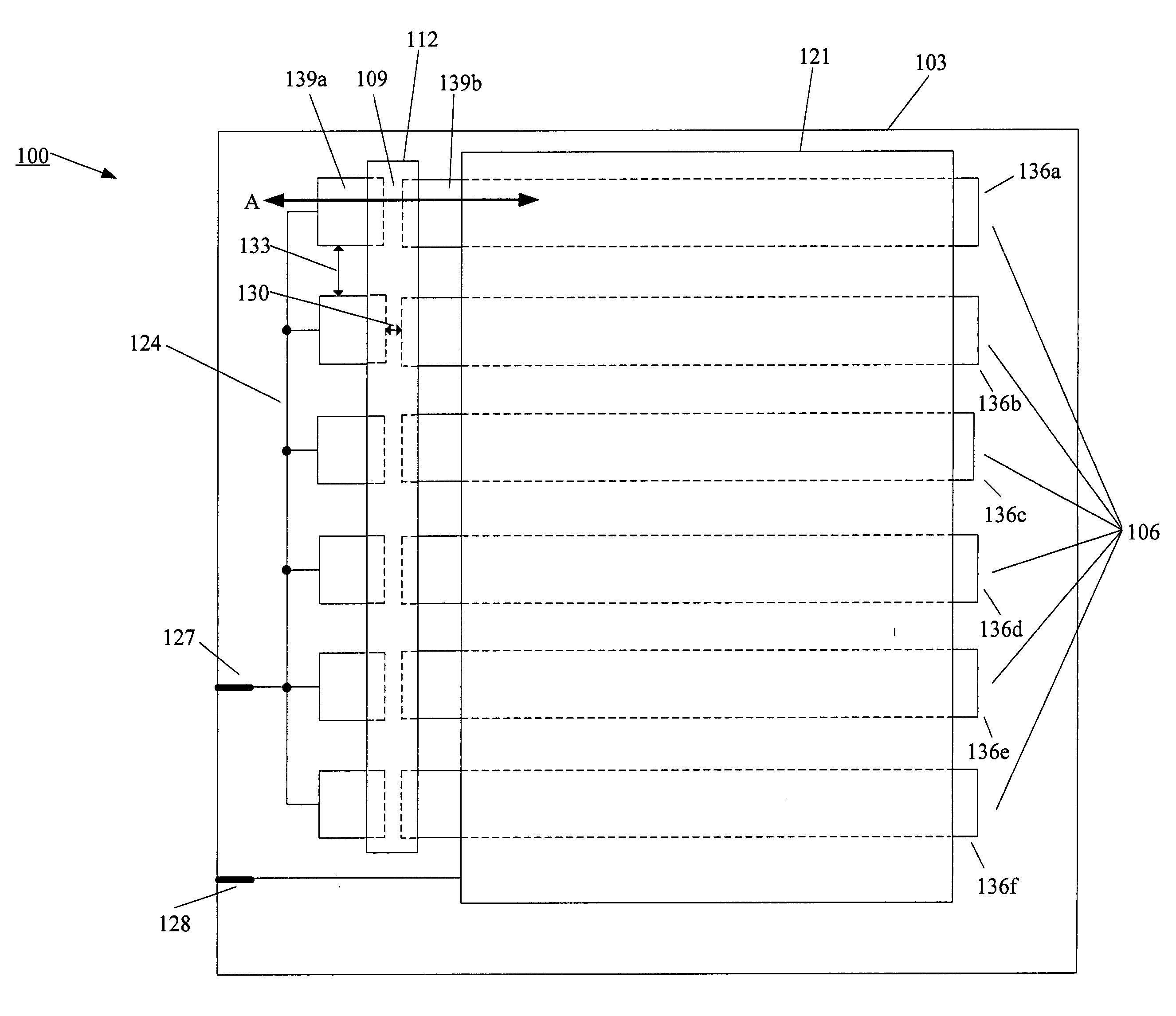
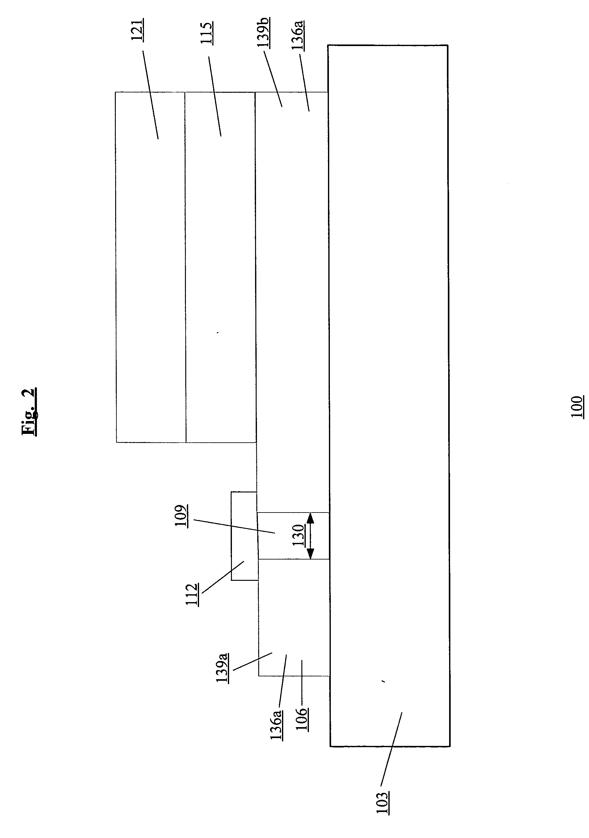
[0041]FIG. 2 shows a cross-section at line A of the OLED lighting device 100 according to the present invention. In FIG. 2, the first electrode 106 is on the substrate 103. The first electrode 106 is patterned into multiple strips and a particular one of these strips include one or more gaps that are on the substrate and located outside the active area of the lighting device. The one or more gaps in a strip segment the strip into two or more strip segments. Specifically, in FIG. 2, the strip 136a includes a gap 109 that segments the strip 136a into a first strip segment 139a and a second strip segment 139b. A fuse material 112 is nonselectively deposited on the first electrode 106 such that it covers the gap 109 and electrically connects the first strip segment 139a and the second strip segment 139b. When the fuse material 112 is nonselectively deposited, then the gap width 130 should be substantially smaller than the distance between adjacent strips so that cross-talk between the a...

second embodiment

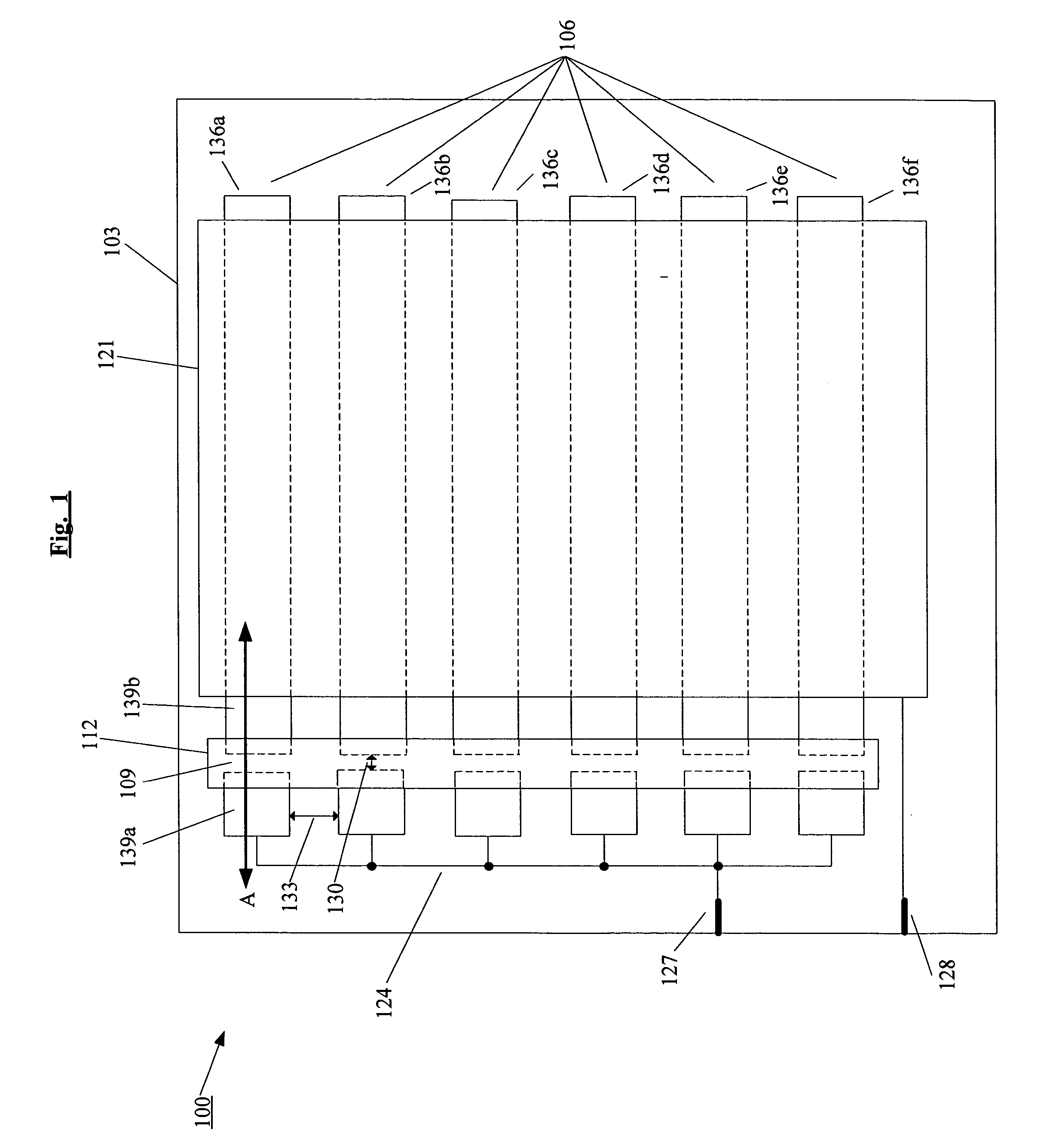
[0042]FIG. 3 shows an OLED lighting device 100 according to the present invention. In this embodiment, a first electrode 106 is on a substrate 103. The first electrode 106 is segmented into multiple strips 136a-f and each of the strips 136a-f has a gap (e.g., strip 136a has a gap 109) that segments the strip into a first segment and a second segment (e.g., the gap 109 segments the strip 136a into a first strip segment 139a and a second strip segment 139b). The gap 109 prevents the flow of electric current between the first strip segment 139a and the second strip segment 139b. In this embodiment, the fuse material 112 is selectively deposited on the gaps so as to cover the gaps and provide an electrical connection between the first strip segments and the corresponding second strip segments. Specifically, in FIG. 3, the fuse material 112 is deposited on the gap 109 so as to provide an electrical connection between the first strip segment 139a and the second strip segment 139b. In this...

third embodiment

[0044]FIG. 5 shows the OLED lighting device 100 according to the present invention. In this embodiment, the first electrode 106 is on the substrate 103. The first electrode 106 is patterned into multiple strips 136a-f and each of the strips 136a-f has a gap (e.g., strip 136a has a gap 109) that segments the particular strip into the first segment and a second segment (e.g., the gap 109 segments the strip 136a into a first strip segment 139a and a second strip segment 139b). The gap 109 prevents the flow of electric current between the first strip segment 139a and the second strip segment 139b. The bank structure 142 is formed on the first electrode 106 and includes the multiple apertures 145a-f. The apertures expose the gaps between the strip segments. For example, the aperture 145a in bank structure 142 exposes the gap 109 between the first strip segment 139a and the second strip segment 139b. The apertures can represent pockets or lines. In this embodiment, the fuse material 112 i...


PUM


Abstract

An embodiment of the present invention pertains to an electroluminescent lighting device for area illumination. The lighting device is fault tolerant due, in part, to the patterning of one or both of the electrodes into strips, and each of one or more of these strips has a fuse formed on it. The fuses are integrated on the substrate. By using the integrated fuses, the number of external contacts that are used is minimized. The fuse material is deposited using one of the deposition techniques that is used to deposit the thin layers of the electroluminescent lighting device.

Description

GOVERNMENT RIGHTS [0001] This invention was made with Government support under Contract No. DE-FC26-04NT41947 awarded by the Department of Energy. The Government has certain rights in the invention.BACKGROUND OF THE INVENTION [0002] The use of OLED panels as a lighting device is desirable—such as for area lighting in the workplace and the home. The OLED lighting device has characteristics that are different than an OLED display and these differences can be exploited to improve reliability and ease of manufacture while reducing cost. For example, electrical shorts are a major concern with OLED devices. A short occurs when any imperfection in the OLED causes its cathode to be in direct contact (or very close proximity) with its anode resulting in an area of much lower resistance than the remaining area between the anode and the cathode. Shorts may occur in any of the layers forming the element and may be caused by, for example, substrate imperfections or asperities, anode layer irregu...

Claims


Application Information

Patent Timeline
Patent Type & Authority Applications(United States)
IPC IPC(8): H05B33/06
CPCH01L27/3225H01L51/50H01L2251/5361H01L51/5203H01L51/5012H10K59/00H10K50/00H10K50/805H10K50/11
Inventor PSCHENITZKA, FLORIAN
Owner OSRAM OLED
Why Eureka
Try Eureka