Semiconductor integrated circuit

a technology of integrated circuits and semiconductors, applied in logic circuits, generating/distributing signals, pulse techniques, etc., can solve the problems of increased mask price, increased difficulty in timing design of signal integrity, and longer diffusion period, so as to reduce the design time

Inactive Publication Date: 2006-03-30
PANASONIC CORP
View PDF28 Cites 13 Cited by
  • Summary
  • Abstract
  • Description
  • Claims
  • Application Information

AI Technical Summary

Benefits of technology

[0014] To solve the above problems, the present invention aims to provide a semiconductor integrated circuit in which a clock signal supplied to each flip-flop will not be adversely affected even when a design of the semiconductor integrated circuit is changed to use a spare flip-flop. The present invention also aims to provide a manufacturing method for such a semiconductor integrated circuit.

Problems solved by technology

The use of a most advanced microfabrication technique in semiconductor integrated circuit design has advantages such as reducing a total semiconductor cost in a product system and allowing a large-scale circuit to be packed on a single semiconductor integrated circuit chip, but also has disadvantages such as a longer diffusion period, a higher mask price, greater difficulty in timing design for signal integrity, and a longer functional inspection period.
This may disturb the balance in timing adjustment of the clock signal supplied to main standard cells used for achieving the original function of the semiconductor integrated circuit.
Also, crosstalk may occur between the new wire and its neighboring signal line, which can further disturb the balance in timing adjustment of the clock signal.
Due to these problems, it is difficult to perform a circuit change without disturbing synchronization.
This makes it impossible to reduce a design time.

Method used


Image

  • Semiconductor integrated circuit
  • Semiconductor integrated circuit
  • Semiconductor integrated circuit

Examples


first embodiment

1. First Embodiment

[0066] The following describes a semiconductor integrated circuit 10 (not illustrated) according to a first embodiment of the present invention. To achieve a desired function, the semiconductor integrated circuit 10 is formed by a plurality of layers including at least one cell placement layers where a plurality of standard cells (such as flip-flops and inverters) are placed, and at least one metal wiring layer. Each cell is connected to another cell and the like, via a signal line formed in the metal wiring layer. The semiconductor integrated circuit 10 is roughly made up of a plurality of functional blocks including a functional block 101.

[0067] The following describes the functional block 101 in the semiconductor integrated circuit 10.

1.1. Construction of the Functional Block 101

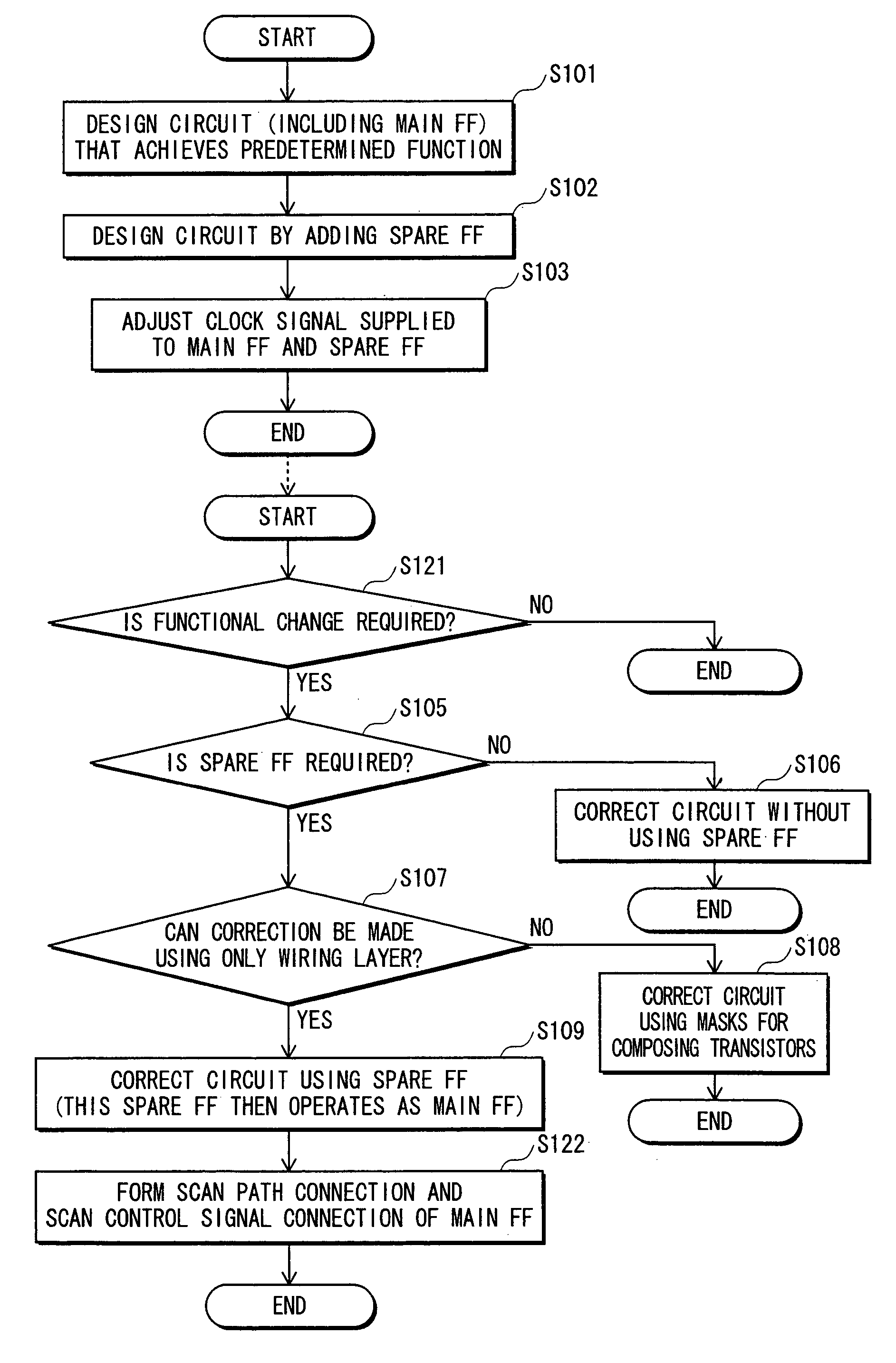
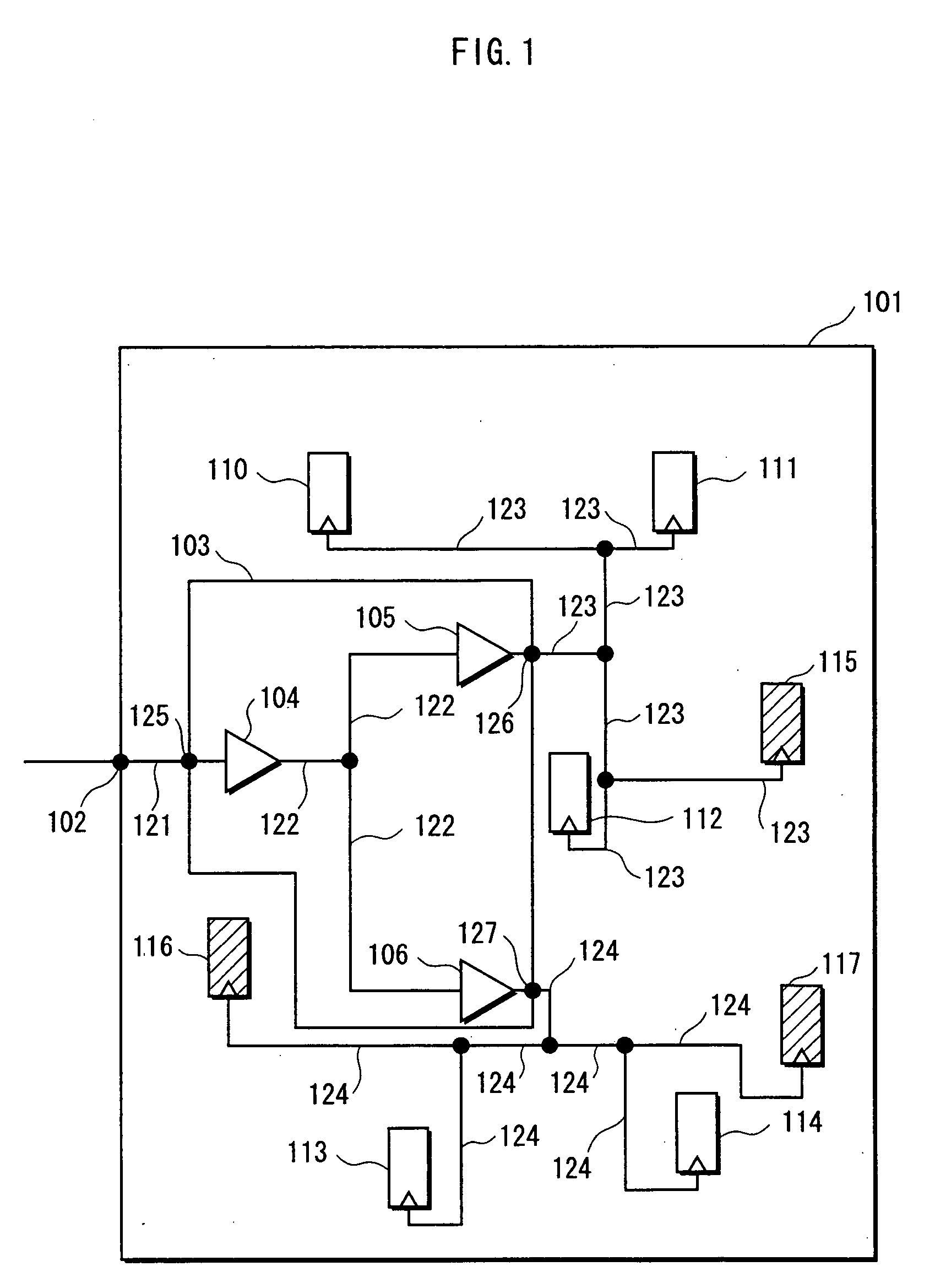
[0068]FIG. 1 is a simplified layout diagram mainly showing a clock-based construction of the functional block 101. Regarding the clock-based construction, the functional block 101 inc...

second embodiment

2. Second Embodiment

[0122] The following describes a semiconductor integrated circuit 30 (not illustrated) according to a second embodiment of the present invention. To achieve a desired function, the semiconductor integrated circuit 30 is formed by a plurality of layers including at least one cell placement layer where a plurality of standard cells (such as flip-flops and inverters) are placed, and at least one metal wiring layer. Each cell is connected to another cell and the like, via a signal line formed in the metal wiring layer. The semiconductor integrated circuit 30 is roughly made up of a plurality of functional blocks including functional blocks 301 and 411.

2.1. Construction of the Functional Block 411

[0123]FIG. 8 is a simplified layout diagram mainly showing a construction of the functional block 411 and a clock-based construction of the functional block 301. As shown in the drawing, the functional block 411 includes an input terminal 364, a clock buffer 353, a signal l...

third embodiment

3. Third Embodiment

[0197] The following describes a semiconductor integrated circuit 50 (not illustrated) according to a third embodiment of the present invention. To achieve a desired function, the semiconductor integrated circuit 50 is formed by a plurality of layers including at least one cell placement layer where a plurality of standard cells (such as flip-flops and inverters) are placed, and at least one metal wiring layer. Each cell is connected to another cell and the like, via a signal line formed in the metal wiring layer. The semiconductor integrated circuit 50 is roughly made up of a plurality of functional blocks including functional blocks 501 and 601.

3.1. Construction of the Functional Block 601

[0198]FIG. 13 is a simplified layout diagram mainly showing a construction of the functional block 601 and a clock-based construction of the functional block 501. In the drawing, the functional block 601 includes an input terminal 651, a clock buffer 507, a signal line 652, c...


PUM


Abstract

To provide a semiconductor integrated circuit in which a clock signal supplied to each flip-flop will not be adversely affected when a functional change is made using a spare flip-flop. The semiconductor integrated circuit includes a plurality of main flip-flops which contribute to a predetermined function, a plurality of spare flip-flops, and a clock tree synthesis circuit that generates a clock signal which is adjusted for synchronizing the plurality of main flip-flops and the plurality of spare flip-flops and supplies the adjusted clock signal to the plurality of main flip-flops and the plurality of spare flip-flops.

Description

[0001] This application is based on applications No. 2004-287056 and 2005-265444 filed in Japan, the contents of which are hereby incorporated by reference. BACKGROUND OF THE INVENTION [0002] 1. Field of the Invention [0003] The present invention relates to a semiconductor integrated circuit in which spare flip-flops are contained beforehand as repair cells. [0004] 2. Related Art [0005] With a rapid expansion of the market of products that carry semiconductor integrated circuits in recent years, the semiconductor integrated circuit products are increasingly diversified and sophisticated and their life cycles are shortening. Under such circumstances, short-term development and high functionality are required of semiconductor integrated circuits. [0006] Also, as semiconductor manufacturing technologies progress, a large-scale circuit previously uncontainable in a single semiconductor integrated circuit chip can now be implemented in a single semiconductor integrated circuit chip throu...

Claims


Application Information

Patent Timeline
Patent Type & Authority Applications(United States)
IPC IPC(8): H03K19/00
CPCG01R31/318583G06F1/10G01R31/318594
Inventor INOUE, GENICHIRO
Owner PANASONIC CORP
Why Eureka
Try Eureka