Method for implementing functional changes into a design layout of an integrated device, in particular a system-on-chip, by means of mask programmable filling cells

a technology of functional changes and design layouts, applied in logic circuits, specific program execution arrangements, program control, etc., can solve the problems of inflexibility, inability to implement a certain type of logic cells, and increasing complexity of integrated circuit scales and designs, etc., to reduce design revision time and cost.

Active Publication Date: 2012-07-03
STMICROELECTRONICS SRL
View PDF27 Cites 10 Cited by
  • Summary
  • Abstract
  • Description
  • Claims
  • Application Information

AI Technical Summary

Benefits of technology

[0023]An object is to provide a method for implementing debug infrastructures in a System-on-Chip (SoC) having structural and functional features allowing for reduced design revision time and costs, overcoming the limitations and the drawbacks of the known debug methods.
[0024]A method is for implementing changes to the functionality of a design layout of an integrated device, in particular a SoC functional changes on its design layout through mask programmable filler cells by way of coarse grain functions. These filler cells are Engineering Change Order (ECO) base cells comprising a first pair of MOS transistors with a common gate and a second pair of MOS transistors with separate gates and having unmodified metal contact layers. In particular, the method uses the filler cells' area to enhance silicon visibility for advanced on-field silicon device validation, debug, and diagnosis.

Problems solved by technology

These demands have made the scales and designs of an Integrated Circuit (IC) increasingly complex and time consuming.
In particular, physical layout takes up a major portion of the cycle of designing an Application Specific Integrated Circuit (ASIC).
However, due to limitations inherent in the software environment, the place-and-route CAD limits uses that these extra logic cells to predefined types and numbers.
Such inflexibility may be undesirable.
For instance, in adding logic elements as used under an ECO, a logic cell of a certain type may not be available for implementing a desired function.
Moreover, it is a painful and time-consuming task to identify the extra logic cells and provide the proper wiring to properly connect the added cells.
Because of the increasing complexity of the IC design and modification, the turn-around time to incorporate the desired ECO changes is generally high.
Nevertheless, such methods are inefficient in terms of area, and in terms of performance for the implementation of debug infrastructures.
Even if this approach has some advantages, it has the drawback of allowing logic changes only by mask modifications.
Moreover, the cell topology and granularity obtained are not optimized for a hardware debug logic implementation.
In particular, this approach with less than optimal cell topology and granularity, causes an area increase of the logic cells, increasing the routing resources needed in the ECO implementation, this being a problem for design development.
As a consequence, the method described above is not efficient in terms of costs and is time consuming.
It is also known that, in spite of huge efforts in design verification, errors are still found in about two thirds of newly manufactured SoCs.
The most recently developed devices however have short market windows, and the delays caused by inefficient and unpredictable debugging significantly increase the time-to-market of such devices, and thus result in a significant loss of market share, or even a complete loss of revenue.
The most commonly used tools for silicon debugging are debuggers for embedded software, but these tools provide only limited observation into the SoC hardware domain, mostly by monitoring processor busses.
However, the DfD structures are design-specific, there are no automatic tools to insert them or process the information they provide, and in general, there is little reuse from project to project.
Moreover, the software used to configure and operate custom instrumentation is often inadequate.
Manual instrumentation of thousands of signals takes a long time, is error-prone, and cannot easily accommodate subsequent design changes.
In essence, ad-hoc methods do not scale well for future designs.
Even if the described approach is advantageous for several aspects, it has the drawback that a new product revision is needed in order to change the used debug structures.

Method used


Image

  • Method for implementing functional changes into a design layout of an integrated device, in particular a system-on-chip, by means of mask programmable filling cells
  • Method for implementing functional changes into a design layout of an integrated device, in particular a system-on-chip, by means of mask programmable filling cells
  • Method for implementing functional changes into a design layout of an integrated device, in particular a system-on-chip, by means of mask programmable filling cells

Examples


Embodiment Construction

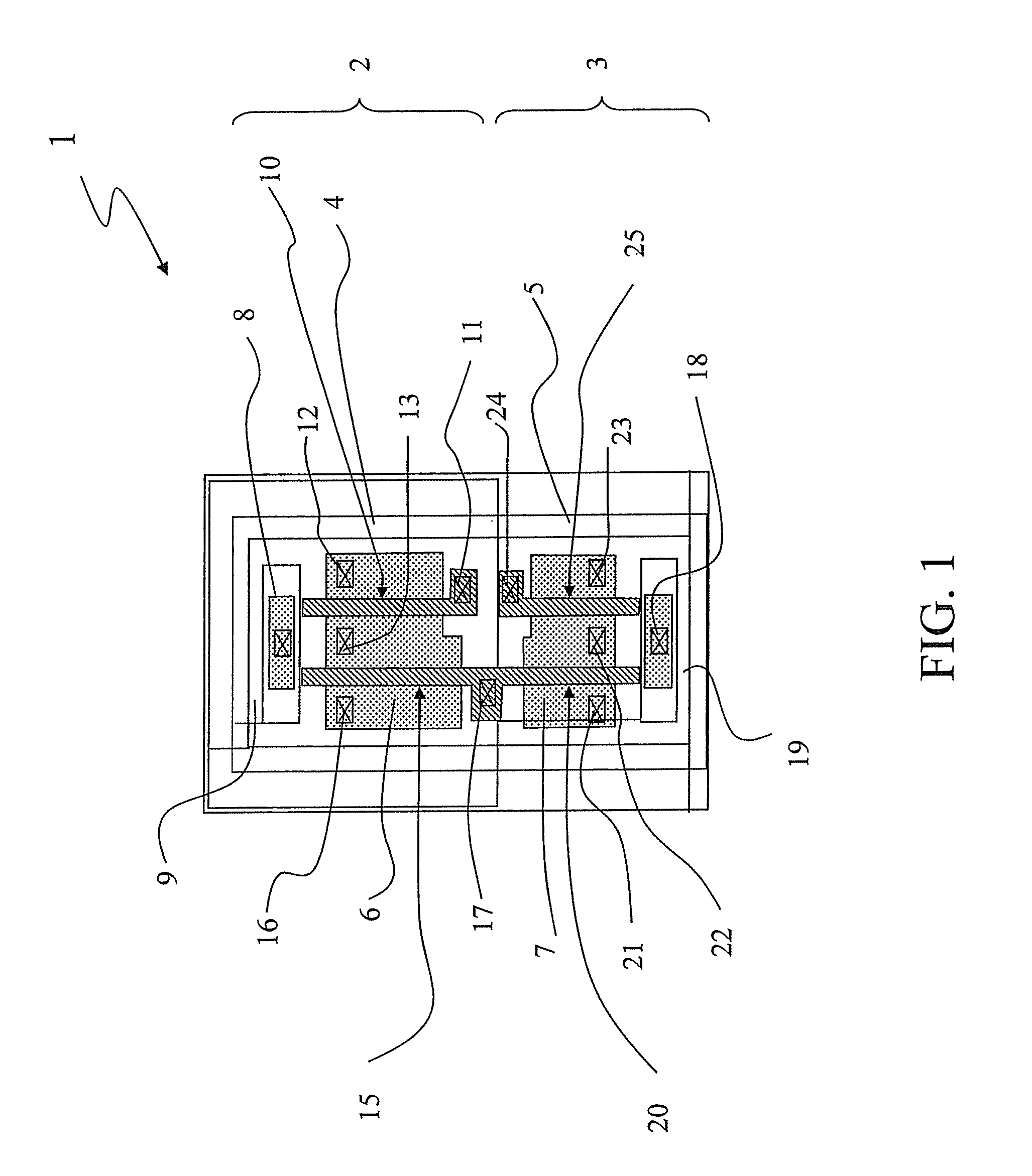
[0037]Referring specifically to FIG. 1, a top view of a layout of an Engineering Change Order (ECO) base cell 1 according to the present invention is shown. It should be noted that the base cell 1 is asymmetrical because of the lack of a virtual center line, with respect to which all patterns of material layers are symmetrically mirrored. In particular, according to this embodiment, the base cell 1 comprises four devices, such as NMOS transistors and PMOS transistors. A P side 2 and an N side 3 are thus defined in the base cell 1.

[0038]In particular, an N-well 4 provides a substrate wherein two PMOS transistors are formed and a P-well 5 provides a substrate wherein two NMOS transistors are formed. A P+ region 6 and an N+ region 7 are implanted on the substrates provided respectively by the N-well 4 and the P-well 5. In particular, the P+ implant of the P+ region 6 forms the source and drain regions of the PMOS transistors, as well as the N+ implant of the N+ region 7 forms the sourc...


PUM


Abstract

A System-on-Chip (SoC) may include logic blocks connected to each other and to external connections, and a hardware debug infrastructure logic connected to the logic blocks and for performing functional changes to a design layout of the SoC. The hardware debug infrastructure logic may include software re-configurable modules based upon the logic blocks obtained from substituting a mask programmable ECO base cell configured as a functional logic cell for a logic cell in the design layout.

Description

FIELD OF THE INVENTION[0001]The present invention relates to a method for implementing changes to the functionality of a design layout of an integrated device, in particular, a System-on-Chip (SoC) through mask-programmable filler cells.[0002]The present invention also relates to a SoC instrumented with debug infrastructure logic which can be used to implement functional changes.BACKGROUND OF THE INVENTION[0003]As is known, demands of consolidating functions and applications from printed circuit board to a single chip are growing stronger. These demands have made the scales and designs of an Integrated Circuit (IC) increasingly complex and time consuming. For this reason, Computer-Aided Design (CAD) has become a useful tool to speed up and improve the quality of IC design. In particular, physical layout takes up a major portion of the cycle of designing an Application Specific Integrated Circuit (ASIC).[0004]In creating a physical layout of an ASIC, a computer layout may be first ge...

Claims


Application Information

Patent Timeline
Patent Type & Authority Patents(United States)
IPC IPC(8): G06F17/50H01L25/00H03K19/173G06F19/00G01R31/28
CPCG06F17/5068G06F30/39
Inventor NARDONE, VALENTINASTUCCHI, STEFANIACICCARELLI, LUCACALI, LORENZO
Owner STMICROELECTRONICS SRL
Why Eureka
Try Eureka