Optical inspection with alternating configurations

Active Publication Date: 2006-03-30
APPL MATERIALS ISRAEL LTD
View PDF4 Cites 45 Cited by
  • Summary
  • Abstract
  • Description
  • Claims
  • Application Information

AI Technical Summary

Benefits of technology

[0012] In some embodiments, the scanning pattern of the irradiated area, the pulse generation, the capturing of the images and the alternation between the two optical configurations are mutually synchronized so that each area of the samp

Problems solved by technology

For example, one of the performance limitations associated with optical inspection systems is the limited dynamic range of the detector elements used for measuring the scattered radiation.
As a result, the dynamic range of the scattered radiation often exceeds the dyn

Method used


Image

  • Optical inspection with alternating configurations
  • Optical inspection with alternating configurations
  • Optical inspection with alternating configurations

Examples


Embodiment Construction

System Description

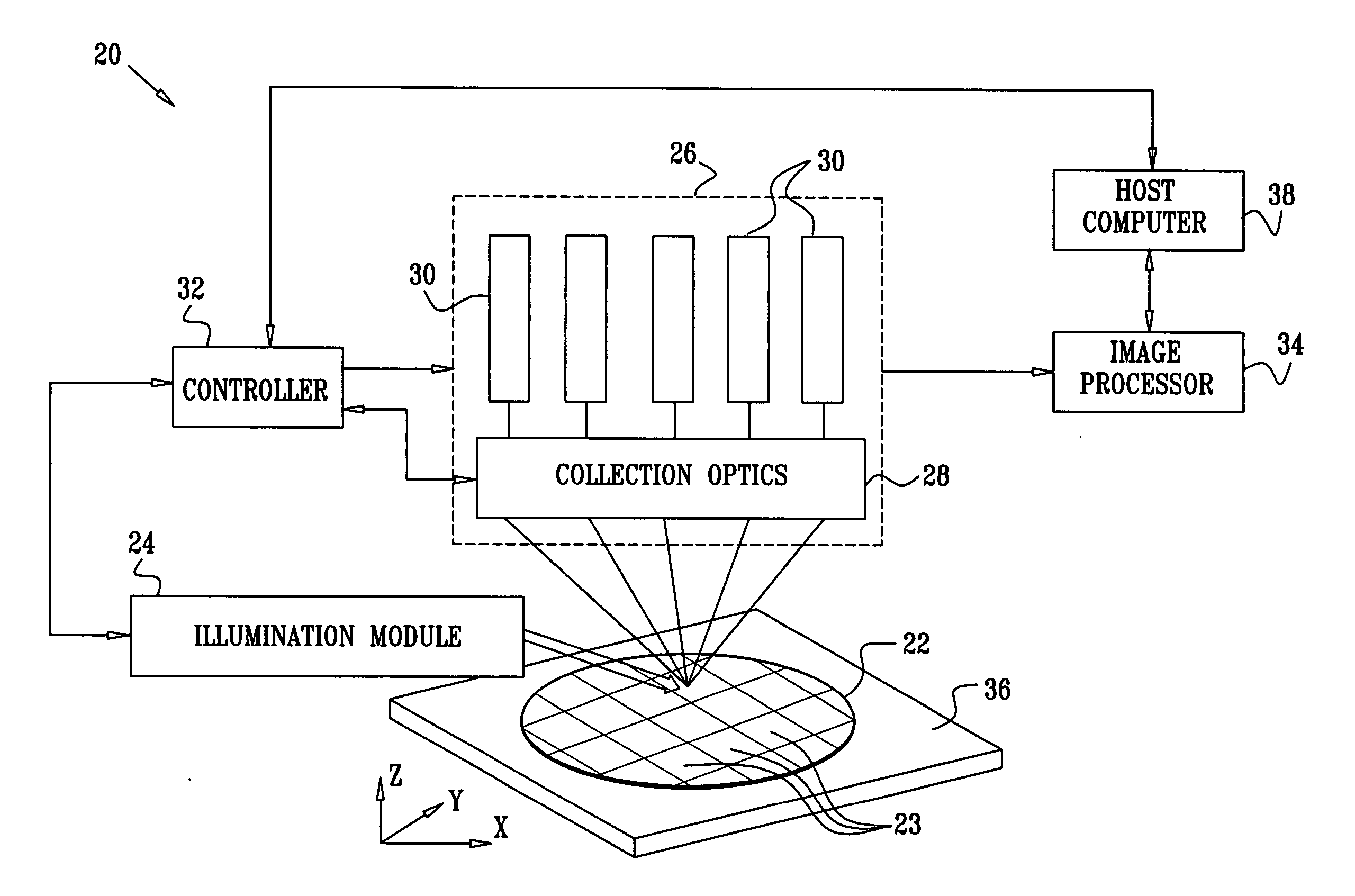
[0042]FIG. 1 is a block diagram that schematically illustrates a system 20 for optical inspection of a sample, such as a semiconductor wafer 22, in accordance with an embodiment of the present invention. Typically, wafer 22 comprises multiple dies 23 of a particular semiconductor device arranged in a repetitive pattern. In some embodiments, wafer 22 is patterned, using any known semiconductor device fabrication process, and system 20 applies dark-field optical techniques to detect defects on the surface of the wafer. Alternatively, the principles of system 20 and the inspection methods described below may also be applied to unpatterned wafers and to inspection of other types of samples and surfaces, such as masks and reticles.

[0043] System 20 comprises an illumination module 24, which irradiates the surface of wafer 22. In some embodiments, module 24 comprises a light source, such as a laser, which emits pulsed laser radiation. In some embodiments, module 24 emi...


PUM


Abstract

An imaging system for inspection of a sample includes an illumination module, which irradiates a surface of the sample with pulsed optical radiation. A mechanical scanner translates at least one of the sample and part of the imaging system so as to scan an area irradiated by the pulsed optical radiation over the surface in order to irradiate successive, partially overlapping frames on the surface by respective successive pulses of the pulsed radiation. A collection module collects the optical radiation scattered from the surface so as to capture a sequence of images of the irradiated frames. A system controller varies a configuration of the imaging system in alternation between at least first and second different optical configurations in synchronization with the pulsed optical radiation.

Description

CROSS-REFERENCE TO RELATED APPLICATION [0001] This application claims the benefit of U.S. Provisional Patent Application 60 / 613,641, filed Sep. 27, 2004. This application is also related to U.S. patent application Ser. No. 10 / 511,092. Both of these related applications are incorporated herein by reference.FIELD [0002] The present invention relates generally to optical inspection, and particularly to methods and systems for detection of features and defects in semiconductor wafers. BACKGROUND [0003] Optical inspection is commonly used in semiconductor device manufacturing to detect defects on the surface of a wafer, such as contaminant particles, scratches and unremoved portions of material layers. Defects can cause device failures, thus substantially reducing the process yield. Therefore, careful inspection is required to verify the cleanliness and quality both of unpatterned wafers and of patterned wafers at various stages of the manufacturing process. [0004] A common method for in...

Claims


Application Information

Patent Timeline
IPC IPC(8): G01N21/88
CPCG01N21/9501G01N2021/479G01N21/956
Inventor GUETTA, AVISHAYKORNGUT, DORONSHOHAM, DORONPINKAS, IDDOEYNAT, RONEN
Owner APPL MATERIALS ISRAEL LTD
Why Eureka
Try Eureka