Differential Imaging For Single-Path Optical Wafer Inspection

a technology of optical wafers and imaging, applied in image enhancement, instruments, image data processing, etc., can solve the problems of noise in the collected wafer image, irregularities detected in the wafer image, and noise introduced, so as to reduce memory requirements and compute time, and enhance the detection of defects of some objects

Active Publication Date: 2020-06-25
KLA TENCOR TECH CORP
View PDF0 Cites 3 Cited by
  • Summary
  • Abstract
  • Description
  • Claims
  • Application Information

AI Technical Summary

Benefits of technology

[0011]In another aspect, a semiconductor wafer inspection system includes an image combining device that generates a composite image based on the signals associated with each independent image of the measured area. In some embodiments, the image combining device generates the composite image on a pixel by pixel basis to minimize memory requirements and compute...

Problems solved by technology

Irregularities detected in the wafer image are caused by defects in the periodic structure of the wafer.
The collected wafer image is affected by noise and is therefore never perfectly periodic.
Some of the noise is introduced by imperfections of the wafer inspection tool.
In addi...

Method used


Image

  • Differential Imaging For Single-Path Optical Wafer Inspection
  • Differential Imaging For Single-Path Optical Wafer Inspection
  • Differential Imaging For Single-Path Optical Wafer Inspection

Examples


Embodiment Construction

[0019]Reference will now be made in detail to background examples and some embodiments of the invention, examples of which are illustrated in the accompanying drawings.

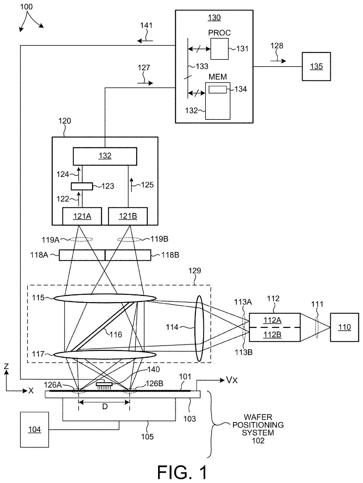
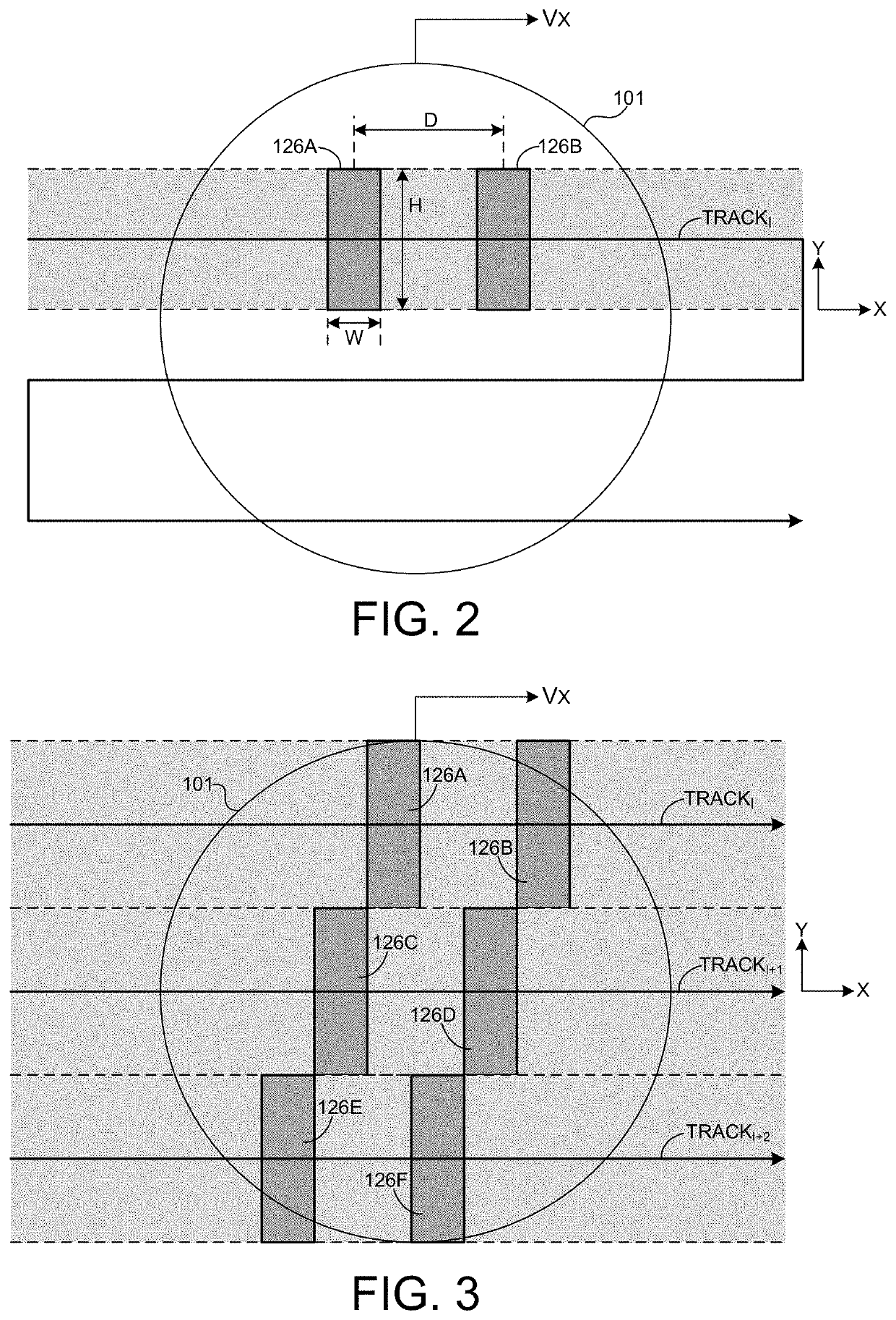
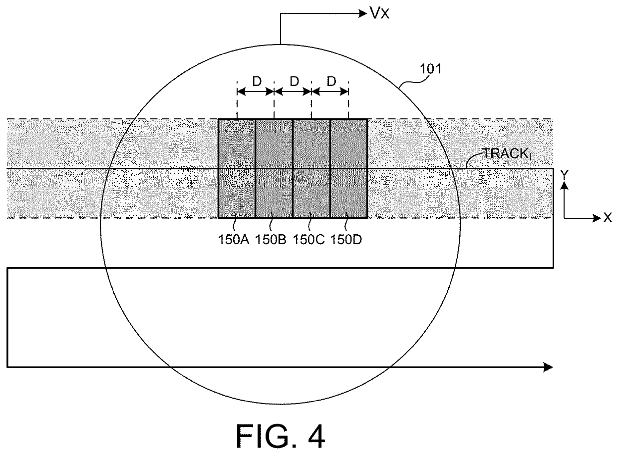
[0020]Methods and systems for enhancing optical wafer inspection without sacrificing measurement throughput are described herein. In one aspect, the area of a wafer under measurement is measured by at least two imaging detectors at different times and a composite image is generated based on the collected images. In some embodiments, the composite image is based on a difference between the collected images. Multiple images of the same measurement area increases signal information that allows improved separation between DOI and nuisance defects. The time between measurements is at least 100 microseconds and no more than 10 milliseconds. By maintaining a short, fixed time between imaging of a particular wafer location with each detector, noise induced by the measurement system itself is minimized. For example, unmodelled...


PUM


Abstract

Methods and systems for enhanced defect detection based on images collected by at least two imaging detectors at different times are described. In some embodiments, the time between image measurements is at least 100 microseconds and no more than 10 milliseconds. In one aspect, one or more defects of interest are identified based on a composite image of a measured area generated based on a difference between collected images. In a further aspect, measurement conditions associated with the each imaged location are adjusted to be different for measurements performed by at least two imaging detectors at different times. In some embodiments, the measurement conditions are adjusted during the time between measurements by different imaging detectors. Exemplary changes of measurement conditions include environmental changes at the wafer under measurement and changes made to the optical configuration of the inspection system.

Description

TECHNICAL FIELD[0001]The described embodiments relate to systems for surface inspection, and more particularly to differential imaging for optical wafer inspection.BACKGROUND INFORMATION[0002]Semiconductor devices such as logic and memory devices are typically fabricated by a sequence of processing steps applied to a substrate or wafer. The various features and multiple structural levels of the semiconductor devices are formed by these processing steps. For example, lithography among others is one semiconductor fabrication process that involves generating a pattern on a semiconductor wafer. Additional examples of semiconductor fabrication processes include, but are not limited to, chemical-mechanical polishing, etch, deposition, and ion implantation. Multiple semiconductor devices may be fabricated on a single semiconductor wafer and then separated into individual semiconductor devices.[0003]Inspection processes are used at various steps during a semiconductor manufacturing process ...

Claims


Application Information

Patent Timeline
IPC IPC(8): G06T7/00G01N21/95G01N21/88
CPCG01N21/9501G06T2207/30148G01N21/8806G06T7/001G06T5/003G06T5/50G06T2207/10148G06T2207/10152G06T2207/20224
Inventor SHCHEMELININ, ANATOLYBEZEL, ILYASHIFRIN, EUGENE
Owner KLA TENCOR TECH CORP
Why Eureka
Try Eureka