Defect location identification for microdevice manufacturing and test

a technology for micro-devices and locations, applied in the direction of instruments, symbolic schematics, cad techniques, etc., can solve problems such as unintended physical aberration, micro-circuits to operate incorrectly or even fail, and become more difficult to manufactur

Inactive Publication Date: 2006-03-30
MENTOR GRAPHICS CORP
View PDF35 Cites 88 Cited by
  • Summary
  • Abstract
  • Description
  • Claims
  • Application Information

AI Technical Summary

Benefits of technology

[0019] Advantageously, various examples of the invention provide tools and techniques for predicting locations at which defects in a microdevice are more likely to occur. Using this information, the tool may identify both a type of defect and the specific circuit portions in which that defect is more likely to occur. This information may then be provided to a test circuit generation tool and/or an automatic test pattern generation tool. For example, various embodiments of the invention may provide a test circuit generation tool or automatic test pattern generation tool with netlist names identifying the netlists corresponding to the portions of the circuit more likely to have a defect upon manufacture. Some embodiments of the invention may also provide the test circuit generation tool and/or an automatic test pattern generation tool with the types of defects that are more likely to

Problems solved by technology

As microdevices become more complex, they also become more difficult to manufacture.
A conventional microcircuit device, for example, may have many millions of connections, and each connection may cause the microcircuit to operate incorrectly or even fail if the connection is not properly made.
It should be noted that some of ordinary skill in the art sometimes make a distinction between a “defect” that occurs when a specific unintended element accidentally introduced into the manufacturing process (such as a mote of dust or another particle) creates an unintended physical aberration, and the type of error that occurs when intended elements of the circuit are simply incorrectly fabricated.
Similarly, some of ordinary skill in the art may sometimes distinguish defects caused by unintended elements introduced during the manufacturing process from post-manufacturing problems with a microdevice, such as when a sub-standard wire shorts out under operation, causing an electrical fault and therefore becoming the source for an electrical “defect” in operation.
As used throughout this specification, however, the term “defect”encompasses any unintended physical aberration in a microdevice, and makes no distinction between environmental or particle related de

Method used


Image

  • Defect location identification for microdevice manufacturing and test
  • Defect location identification for microdevice manufacturing and test
  • Defect location identification for microdevice manufacturing and test

Examples


Embodiment Construction

[0031] Overview

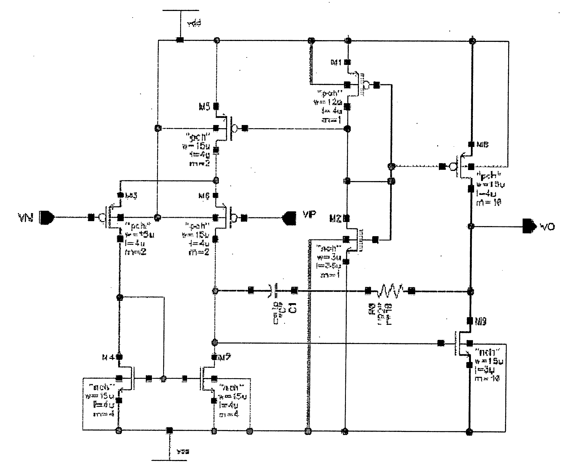
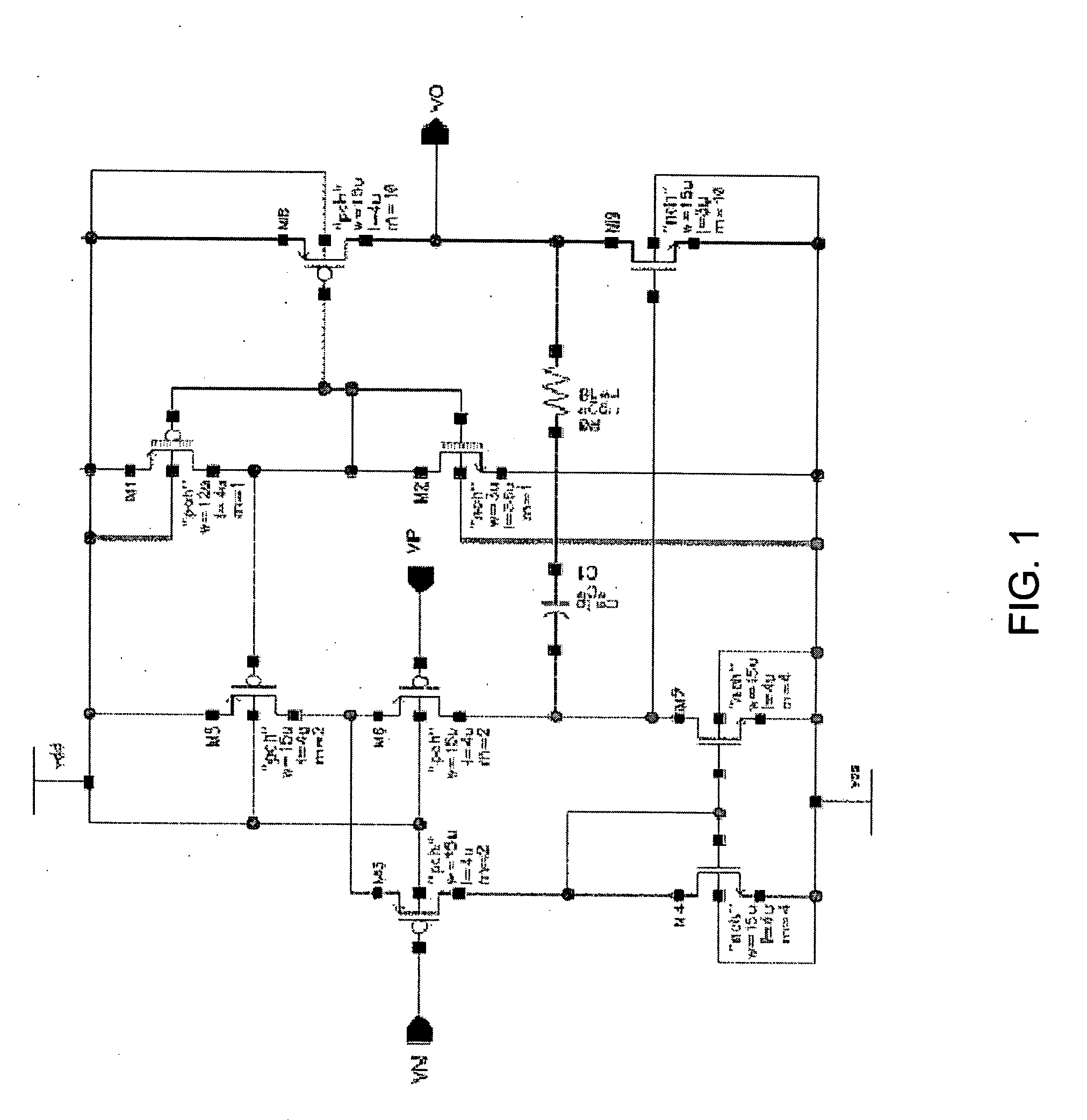
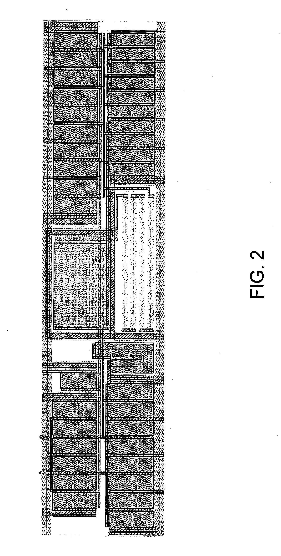
[0032] Different embodiments of the invention are directed to various tools and techniques that assist a manufacturing in developing tests for testing manufactured microdevices. As used herein, the term microdevice includes any device having physical features of 100 micrometers or less in size, including, but not limited to, microcircuits, thin film structures such as magnetic disk drive heads, gene chips, and microelectromechanical systems (MEMS).

[0033] According to different embodiments of the invention, a defect identification tool is employed to predict locations at which defects in a microdevice are more likely to occur. The tool may identify both a type of defect and the circuit location (by, e.g. naming the particular netlist or netlists corresponding to the circuit location) at which that defect is more likely to occur. A test circuit generation tool can then subsequently use this defect information to generate a test circuit that tests for the defect in the...


PUM


Abstract

A defect identification tool is disclosed that predicts locations at which defects in a microdevice are most likely to occur. The tool may identify both a type of defect and the particular netlists in which that defect is likely to occur. A test circuit generation tool can then subsequently use this defect information to generate a test circuit that tests for the defect in the identified portions of the microcircuit. Similarly, an automatic test pattern generation tool may use the defect location information to generate test data custom-tailored to check for faults corresponding to the identified defect in the specified portions of the microcircuit. Various implementations of the tool may be used both to identify the locations at which defects caused by systematic errors, such as manufacturing process deficiencies or flaws, are most likely to occur and the locations at which randomly-created defects are most likely to occur.

Description

[0001] This application is a continuation application of provisional U.S. Application No. 60 / 569,747, filed May 9, 2004, entitled “Defect Location Identification For Microdevice Manufacturing and Test” and naming Joseph D. Sawicki, John G. Ferguson, Sanjay Dhar, Juan Andres Torres Robles, and Janusz E. Rajski, as inventors, which provisional patent application is incorporated entirely herein by reference.FIELD OF THE INVENTION [0002] The present invention relates to various techniques and tools to assist in the design and testing of microdevices. Various aspects of the present invention are particularly applicable to the identification of potential defect locations in a manufactured microdevice from the microdevice's design. BACKGROUND OF THE INVENTION [0003] Microcircuit devices have become commonly used in a variety of products, from automobiles to microwaves to personal computers. As the importance of these devices grows, manufacturers continue to improve these devices. Each year...

Claims


Application Information

Patent Timeline
IPC IPC(8): G06F11/00G01R31/3183G06F9/455G06F17/50
CPCG01R31/318357G06F11/263G06F2217/74G06F2217/14G06F17/50G06F30/00G06F30/333G06F2111/12
Inventor SAWICKI, JOSEPH D.FERGUSON, JOHN G.DHAR, SANJAYROBLES, JUAN ANDRES TORRESRAJSKI, JANUSZ
Owner MENTOR GRAPHICS CORP
Why Eureka
Try Eureka