Electronic device manufacture

a technology of electronic devices and manufacturing methods, applied in the field of electronic device manufacturing, can solve the problems of high capacitance loss, severe processing, cost and material problems, and high cross-talk and capacitance loss,

Inactive Publication Date: 2006-04-06
ROHM & HAAS ELECTRONICS MATERIALS LLC
View PDF12 Cites 12 Cited by
  • Summary
  • Abstract
  • Description
  • Claims
  • Application Information

AI Technical Summary

Benefits of technology

[0009] Also provided by the present invention is an electronic device including a substrate, a metal line-containing layer including an air gap region and a low-k dielectric material region, and a permeable overlayer disposed on the metal line-containing layer, wherein the metal line-containing layer includes a dense packing of metal lines within the air gap region.

Problems solved by technology

Such reduced spacing between metal lines results in an increase in capacitive coupling between nearby conductive traces causing problems such as greater cross-talk and higher capacitive losses.
However, low-k materials have not been used in all applications as they can possess severe processing, cost and materials problems.
The air gap forming techniques that have been developed have varying degrees of complexity but typically employ a material disposed between metal lines that is subsequently removed to provide an air gap.
However, these techniques are not without problems.
This approach presents problems when used with spin-on techniques.
Yet another problem arises if the photosensitive material remaining on the substrate has a high dielectric constant as the effective dielectric constant of the total dielectric stack will be increased.

Method used


Image

  • Electronic device manufacture
  • Electronic device manufacture
  • Electronic device manufacture

Examples


Embodiment Construction

[0017] As used throughout this specification, the following abbreviations shall have the following meanings, unless the context clearly indicates otherwise: ° C.=degrees centigrade; μm=micrometer; UV=ultraviolet; nm=nanometer; and % wt=% by weight.

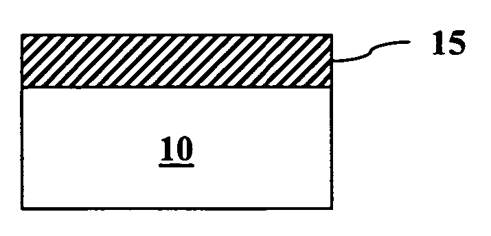
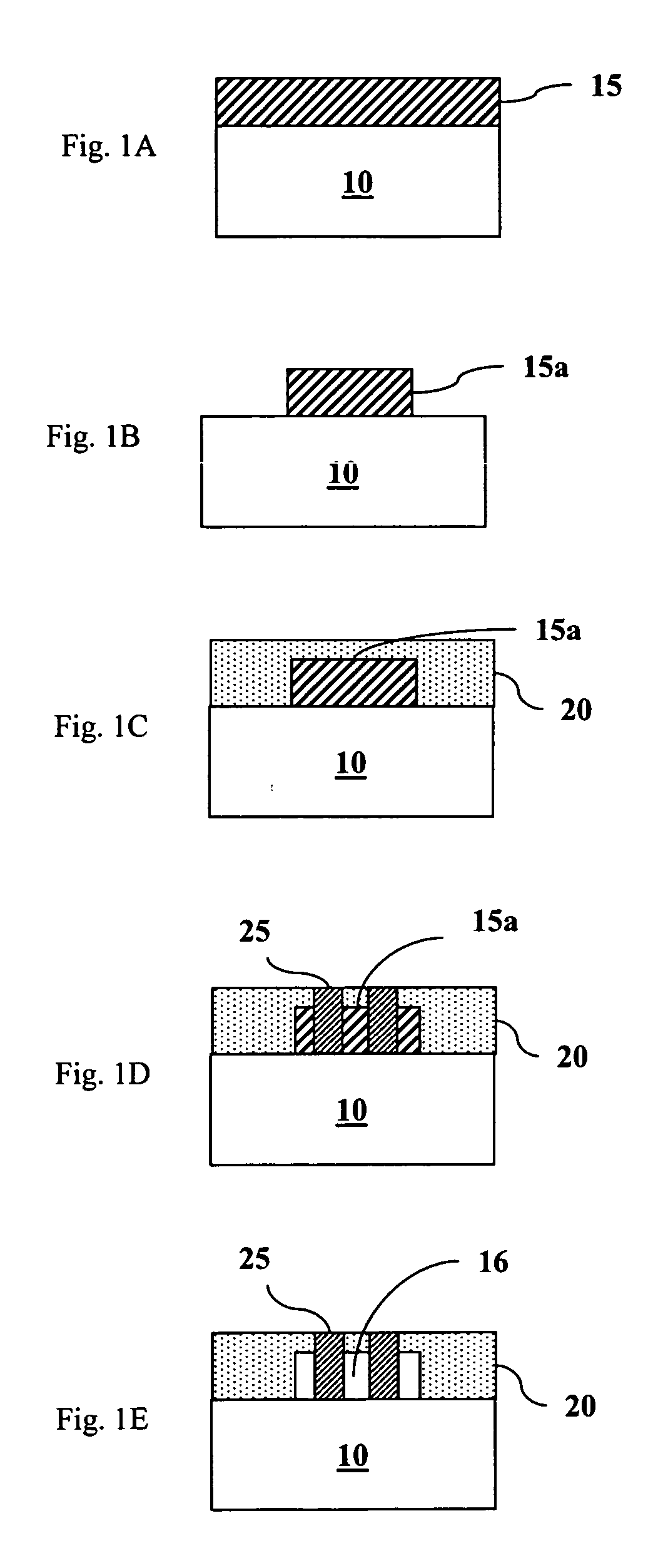
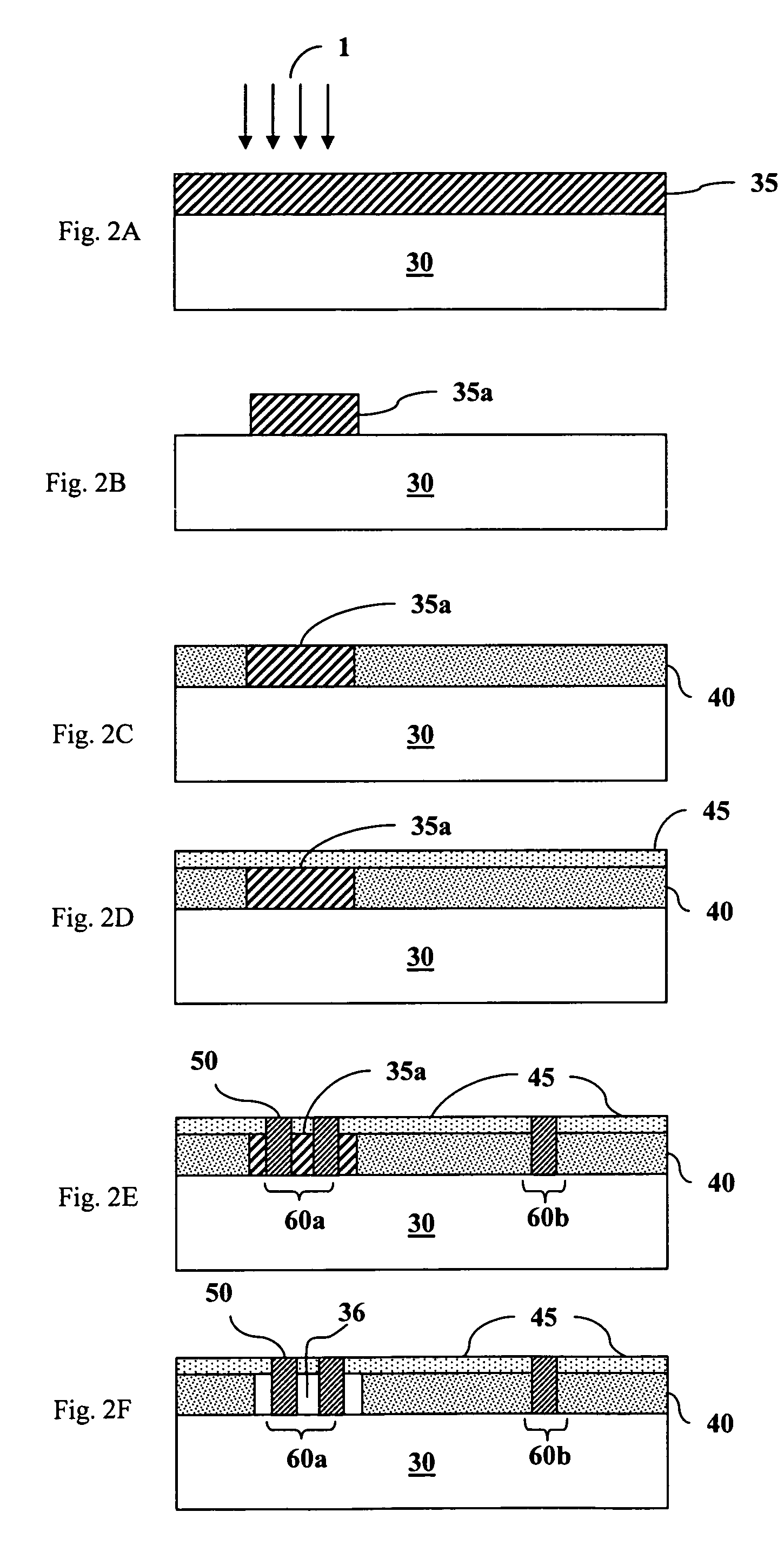
[0018] The term “porogen” refers to any removable material added to a dielectric material as a pore forming material, that is a material such as polymeric particles dispersed in a dielectric material that is subsequently removed to yield pores in the dielectric material. The term “pore” refers to voids formed in the dielectric material. “Low-k dielectric material” refers to any dielectric material having a dielectric constant of ≦3. An “air gap” refers to an closed interior volume containing air (or vacuum) within an electronic device but does not include a “pore”. As used throughout the specification, “feature” refers to the geometries on a substrate. “Apertures” refer to recessed features, such as vias and trenches.

[0019] The term “(me...


PUM

PropertyMeasurementUnit
dielectric constantsaaaaaaaaaa
dielectric constantaaaaaaaaaa
mean particle sizeaaaaaaaaaa

Abstract

Electronic devices having a metal line-containing layer including an air gap region and a low-k dielectric material region where the air gap region includes a dense packing of metal lines is provided. Methods of forming such electronic devices are also provided.

Description

BACKGROUND OF THE INVENTION [0001] The present invention relates generally to the field of electronic device manufacture. More particularly, the present invention relates to the manufacture of integrated circuits using air gaps to reduce capacitive coupling between conductors in such devices. [0002] Advances in integrated circuit technology have reduced the spacing between the metal lines on any given plane of an integrated circuit. Such reduced spacing between metal lines results in an increase in capacitive coupling between nearby conductive traces causing problems such as greater cross-talk and higher capacitive losses. [0003] Low dielectric constant (“low-k”) materials (typically having dielectric constants of approximately 1.8 to 2.5) are being developed as a replacement for conventional dielectric materials used between conductors on a given layer and between layers. These low-k materials reduce capacitive coupling between the conductors as compared to conventional dielectric ...

Claims


Application Information

Patent Timeline
Patent Type & Authority Applications(United States)
IPC IPC(8): G03F7/00
CPCH01L21/7682H01L21/76829
Inventor GALLAGHER, MICHAEL K.
Owner ROHM & HAAS ELECTRONICS MATERIALS LLC
Why Eureka
Try Eureka