Method of manufacturing a substrate with through electrodes

a manufacturing method and technology of through electrodes, applied in the direction of printed circuit manufacturing, printed element electric connection formation, basic electric elements, etc., can solve the problems of warping of the semiconductor substrate, inflicting damage on the semiconductor elements, and varied thickness of the through electrodes in the substra

Inactive Publication Date: 2006-04-06
SHINKO ELECTRIC IND CO LTD
View PDF7 Cites 107 Cited by
  • Summary
  • Abstract
  • Description
  • Claims
  • Application Information

AI Technical Summary

Benefits of technology

[0013] It is an object of the present invention to provide a method of manufacturing a substrate with through el...

Problems solved by technology

However, in the first method of manufacturing such substrate, such a problem exists that heights of the through electrodes are varied in the substrate upon forming the through electrodes by the electroplating.
In this case, when semiconductor elemen...

Method used


Image

  • Method of manufacturing a substrate with through electrodes
  • Method of manufacturing a substrate with through electrodes
  • Method of manufacturing a substrate with through electrodes

Examples


first embodiment

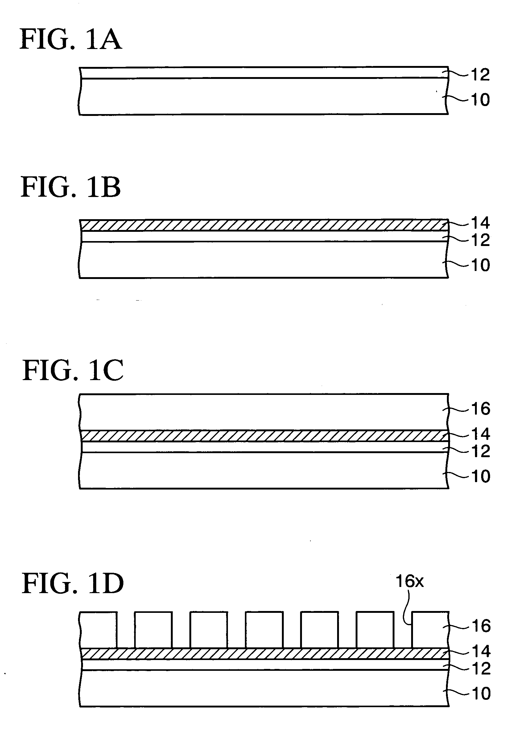
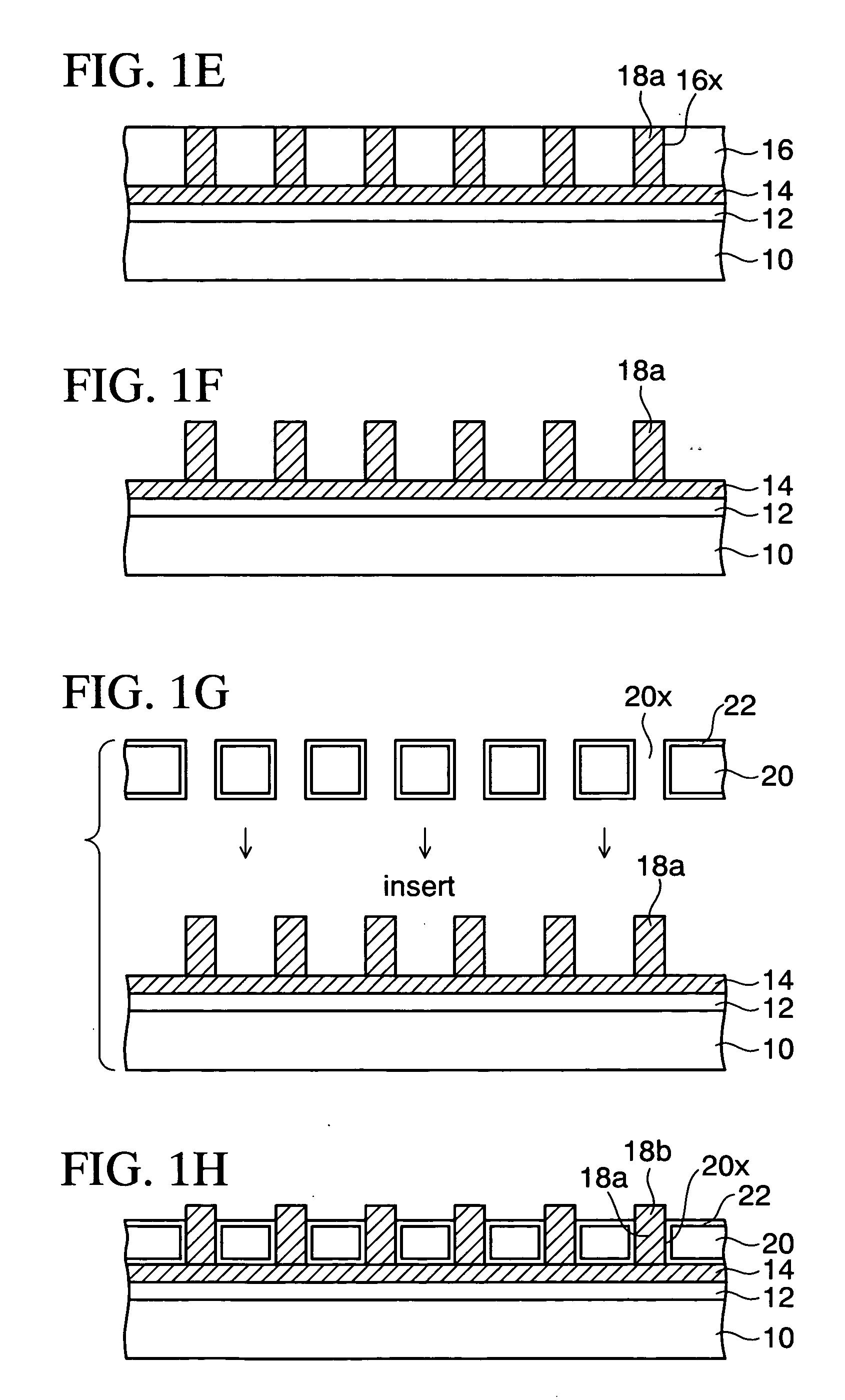
[0027]FIGS. 1A to 1L are sectional views showing a method of manufacturing a substrate with through electrodes according to a first embodiment of the present invention in sequence. In the method of manufacturing the substrate with through electrodes in the first embodiment, as shown in FIG. 1A, first a temporal substrate 10 is prepared, and a peelable layer 12 is formed on the temporal substrate 10. As the temporal substrate 10, a semiconductor substrate (a silicon wafer, a silicon chip, or the like) is used preferably. As the peelable layer 12, a heat peeled tape having such a characteristic that can be pasted onto a seed metal layer formed on the temporal substrate 10 and the peelable layer 12 at an ordinary temperature but can be peeled from an interface of the seed metal layer by applying heat is used preferably.

[0028] Then, as shown in FIG. 1B, a seed metal layer 14 is formed on the peelable layer 12. As the seed metal layer 14, a metallic foil made of copper (Cu), or the like...

second embodiment

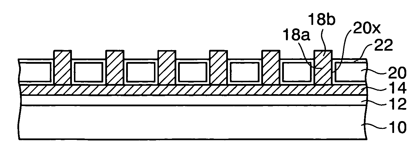
[0051]FIGS. 4A to 4F are sectional views showing a method of manufacturing a substrate with through electrodes according to a second embodiment of the present invention. In the second embodiment, such a mode is shown that the substrate with through electrodes of the present invention is applied to the MEMS (Micro Electro Mechanical Systems) device packaging substrate (silicon cap).

[0052] In the method of manufacturing the substrate with through electrodes of the second embodiment, as shown in FIG. 4A, first the peelable layer 12 and the seed metal layer 14 are formed on the temporal substrate 10 by the same method as the first embodiment, and the metal posts 18a which stand upright are formed on the seed metal layer 14. Then, as shown in FIG. 4B, the semiconductor substrate 20 in which the through holes 20x are provided is prepared, and then the insulating layer 22 is formed on both surfaces of the semiconductor substrate 20 and inner surfaces of the through holes 20x. In the secon...


PUM


Abstract

A method of manufacturing a substrate with through electrodes of the present invention, includes the steps of forming a metal post over a temporal substrate in a state that the metal post is peelable from the temporal substrate, placing a normal substrate in which a through hole is provided in a position corresponding to the metal post over the temporal substrate, whereby inserting the metal post on the temporal substrate into the through hole in the normal substrate, and obtaining a through electrode that is formed of the metal post passing through the normal substrate by peeling the temporal substrate from the metal post.

Description

CROSS-REFERENCE TO RELATED APPLICATIONS [0001] This application is based on and claims priority of Japanese Patent Application No. 2004-290142 filed on Oct. 1, 2004, the entire contents of which are incorporated herein by reference. BACKGROUND OF THE INVENTION [0002] 1. Field of the Invention [0003] The present invention relates to a method of manufacturing a substrate with through electrodes and, more particularly, a method of manufacturing a substrate with through electrodes having such a structure that upper and lower sides of the substrate can be connected electrically via the through electrodes passing through the substrate in a thickness direction. [0004] 2. Description of the Related Art [0005] In the prior art, there is provided a substrate with through electrodes having the structure in which the through electrodes are formed in the substrate along a thickness direction to connect electrically upper and lower sides of the substrate. In Patent Literature 1 (Patent Applicatio...

Claims


Application Information

Patent Timeline
IPC IPC(8): H01L21/44
CPCH01L21/486H01L2224/16235H01L21/76898H01L23/3128H01L25/0657H01L25/50H01L2224/16225H01L2225/06541H01L2225/06582H01L2924/01078H01L2924/01079H01L2924/15311H05K1/0306H05K3/205H05K3/4038H05K2203/0338H01L2224/16145H01L2924/10253H01L21/6835H01L2924/00H01L24/03H01L24/05H01L2224/0554H01L2224/05573H01L2224/05647H01L2224/13025H01L2924/00014H01L2924/1461H01L2224/05599H01L2224/0555H01L2224/0556H05K3/40H05K3/46
Inventor KOIZUMI, NAOYUKISHIRAISHI, AKINORI
Owner SHINKO ELECTRIC IND CO LTD
Why Eureka
Try Eureka