Capacitive micromachined ultrasonic transducer array with through-substrate electrical connection and method of fabricating same

a micro-machined, ultrasonic technology, applied in the direction of generator/motor, mechanical vibration separation, instruments, etc., can solve the problems of long routing lines and inefficient use of the front side of the silicon substrate surface area, and achieve the effect of improving device performance and improving utilization efficiency of real esta

Inactive Publication Date: 2006-04-13
THE BOARD OF TRUSTEES OF THE LELAND STANFORD JUNIOR UNIV
View PDF6 Cites 109 Cited by
  • Summary
  • Abstract
  • Description
  • Claims
  • Application Information

AI Technical Summary

Benefits of technology

[0008] The CMUT elements in the CMUT array can thus be individually or respectively addressed through the substrate on which the array is formed. This helps to increase the utilization efficiency of the real estate on the front side of the substrate while providing better device performance.
[0009] The embodiments of the present invention also provides a method for fabricating the CMUT device, which comprises forming a plurality of dielectric walls on a front side of a substrate, forming a membrane layer over the dielectric walls, and removing a portion of the substrate. The method may further comprises etching trenches through the substrate from a backside of the substrate. The trenches provide isolation between CMUT elements in the CMUT device and allow addressing the CMUT elements individually or respectively from the backside of the first substrate.

Problems solved by technology

This arrangement makes inefficient use of the surface area on the front side of the silicon substrate, and requires long routing lines to address the CMUT cells, especially for two-dimensional CMUT arrays.

Method used


Image

  • Capacitive micromachined ultrasonic transducer array with through-substrate electrical connection and method of fabricating same
  • Capacitive micromachined ultrasonic transducer array with through-substrate electrical connection and method of fabricating same
  • Capacitive micromachined ultrasonic transducer array with through-substrate electrical connection and method of fabricating same

Examples


Embodiment Construction

)

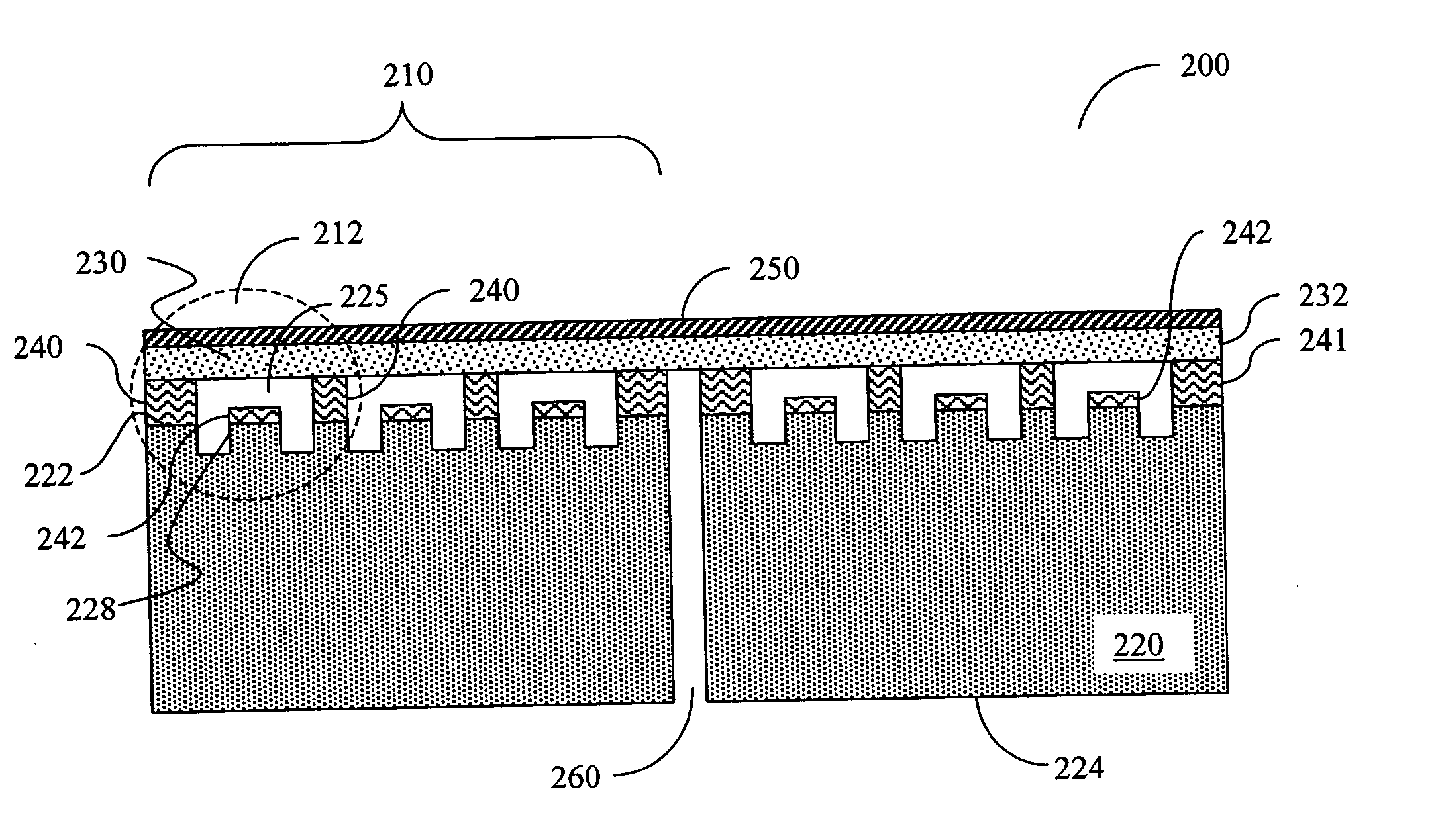
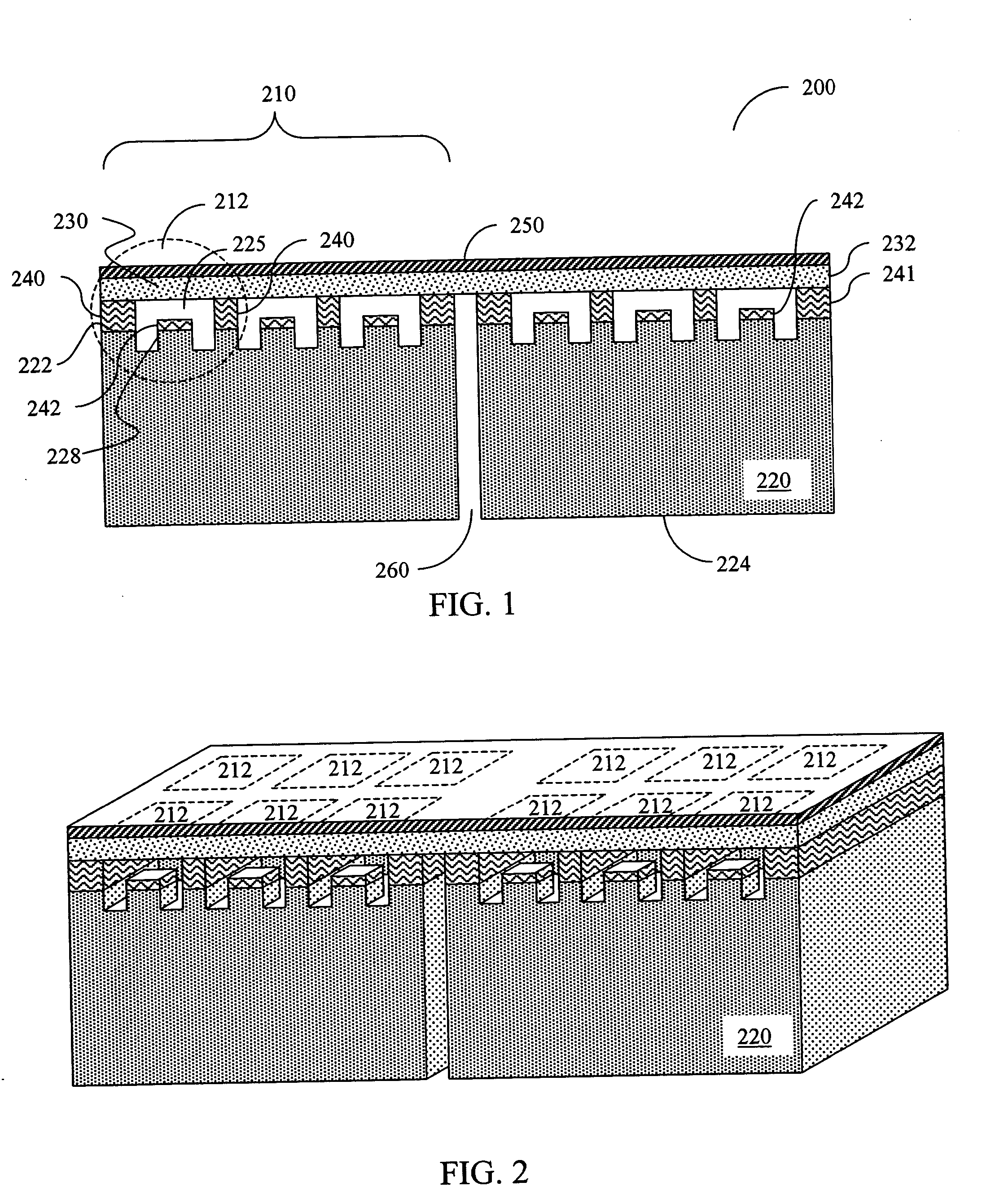
[0019] Referring to FIGS. 2A and 2B, a CMUT array 200 according to one embodiment of the present invention comprises CMUT array elements 210. While FIGS. 2A and 2B each only shows two CMUT array elements 210, it is apparent that a CMUT array in accordance with the present invention can compromise a number of elements arranged in a one or two-dimensional configuration. As shown in FIG. 2A, each array element 210 includes one or more CMUT cells 212 formed on a high conductivity semiconductor substrate 220. Each CMUT cell 212 includes a membrane 230 supported by dielectric walls 240 over a top surface 222 of the substrate 220, and an ultrasonic gap or cavity 225 defined by the membrane 230, the insulating walls 240, and the top surface 222 of the substrate 220. The dielectric walls 240 are part of a first dielectric layer 241 formed over the top surface 222 of the substrate 220, and the membrane 230 is part of a membrane layer 232. An example of the first dielectric layer 241 is a sil...


PUM


Abstract

The embodiments of the present invention provide a CMUT array and method of fabricating the same. The CMUT array has CMUT elements individually or respectively addressable from a backside of a substrate on which the CMUT array is fabricated. In one embodiment, a CMUT array is formed on a front side of a very high conductivity silicon substrate. Through wafer trenches are etched into the substrate from the backside of the substrate to electrically isolate individual CMUT elements formed on the front side of the substrate. Electrodes are formed on the backside of the substrate to individually address the CMUT elements through the substrate.

Description

CROSS REFERENCE TO RELATED APPLICATIONS [0001] The present application claims the benefit of U.S. Provisional Patent Application No. 60 / 577,102 filed on Jun. 4, 2004, the entire content of which is incorporated herein by reference.GOVERNMENT SUPPORT [0002] This invention was made with Government support under Grant No. Navy N00014-02-1-0007 awarded by the Department of the Navy, Office of Naval Research. The Government has certain rights in this invention.FIELD OF THE INVENTION [0003] The present application relates to ultrasonic sensors and actuators, and more particularly to capacitive micromachined ultrasound transducers (CMUT). BACKGROUND OF THE INVENTION [0004] Capacitive micromachined ultrasound transducers (CMUT) have emerged as a viable alternative to traditional piezoelectric transducers. In general, a CMUT is essentially a micron-sized air-gap or vacuum-gap capacitor that, by electrostatic effects, can be used for the generation and detection of acoustic / ultrasonic waves. ...

Claims


Application Information

Patent Timeline
Patent Type & Authority Applications(United States)
IPC IPC(8): G01H11/00
CPCB06B1/0292
Inventor HUANG, YONGLIZHUANG, XUEFENGKHURI-YAKUB, BUTRUS T.CHENG, CHING-HSIANGERGUN, ARIF S.
Owner THE BOARD OF TRUSTEES OF THE LELAND STANFORD JUNIOR UNIV
Why Eureka
Try Eureka