

Ultra shallow junction formation by epitaxial interface limited diffusion
a technology of epitaxial interface and limited diffusion, which is applied in the direction of basic electric elements, electrical apparatus, semiconductor devices, etc., can solve the problems of increasing the difficulty of reducing the oxide thickness (scale the oxide), and the difficulty of obtaining shallower and sharper junctions, so as to increase the oxygen content of the top surface of the silicon substrate, prevent epitaxial growth, and maximize dopant activation
- Summary
- Abstract
- Description
- Claims
- Application Information
AI Technical Summary
Benefits of technology
Problems solved by technology
Method used
Image

Examples
Embodiment Construction
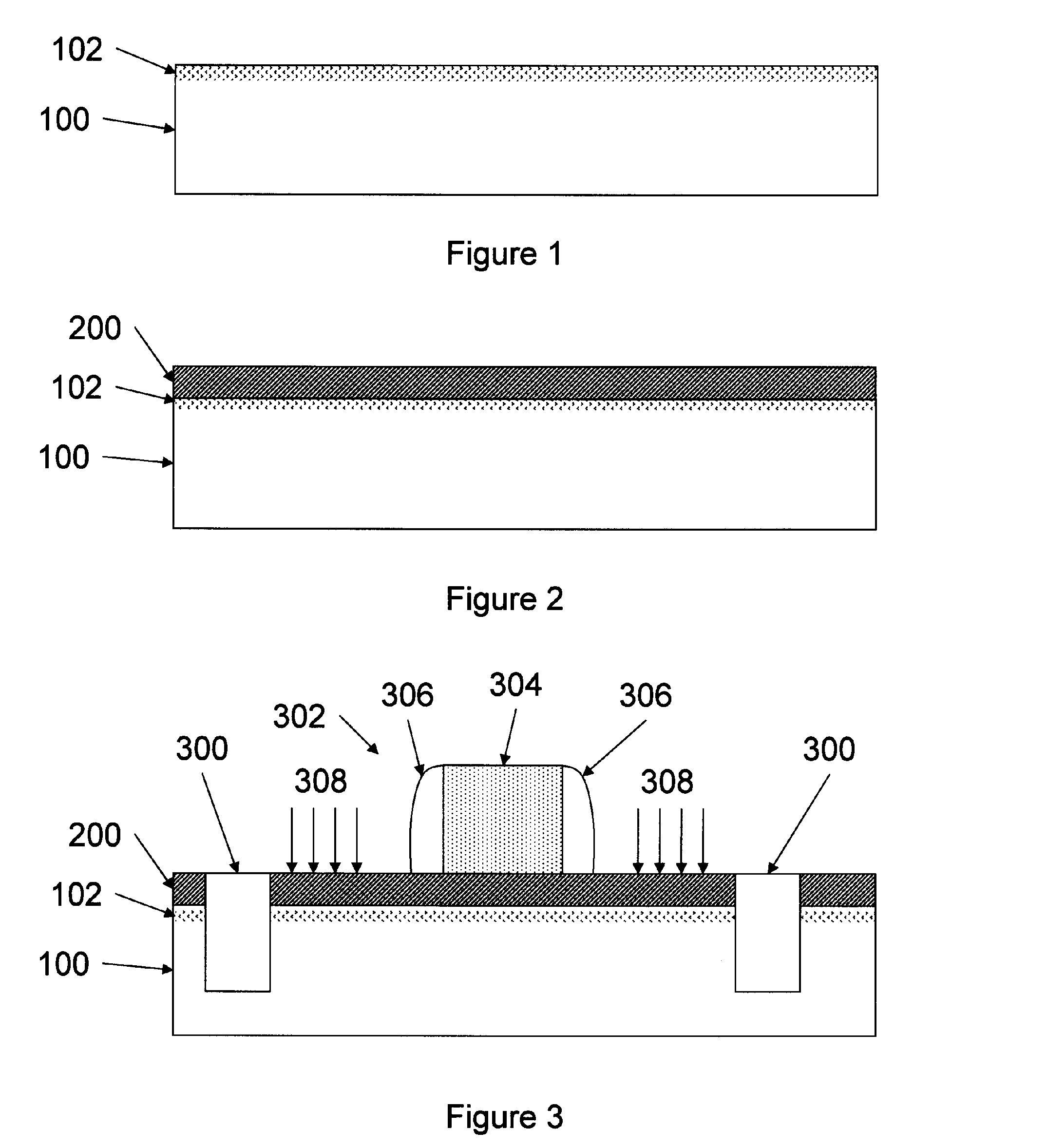
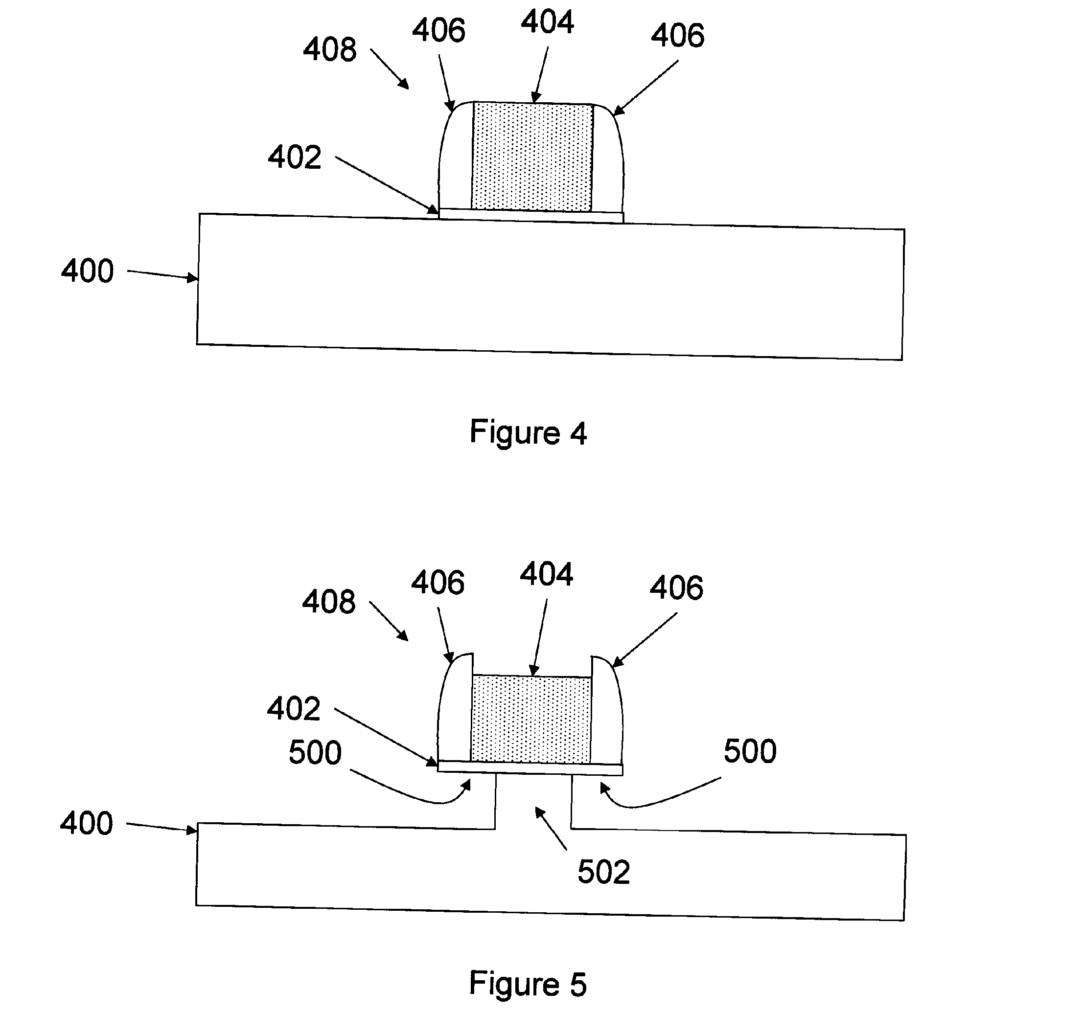
[0020] The present invention and the various features and advantageous details thereof are explained more fully with reference to the nonlimiting embodiments that are illustrated in the accompanying drawings and detailed in the following description. It should be noted that the features illustrated in the drawings are not necessarily drawn to scale. Descriptions of well-known components and processing techniques are omitted so as to not unnecessarily obscure the present invention. The examples used herein are intended merely to facilitate an understanding of ways in which the invention may be practiced and to further enable those of skill in the art to practice the invention. Accordingly, the examples should not be construed as limiting the scope of the invention.
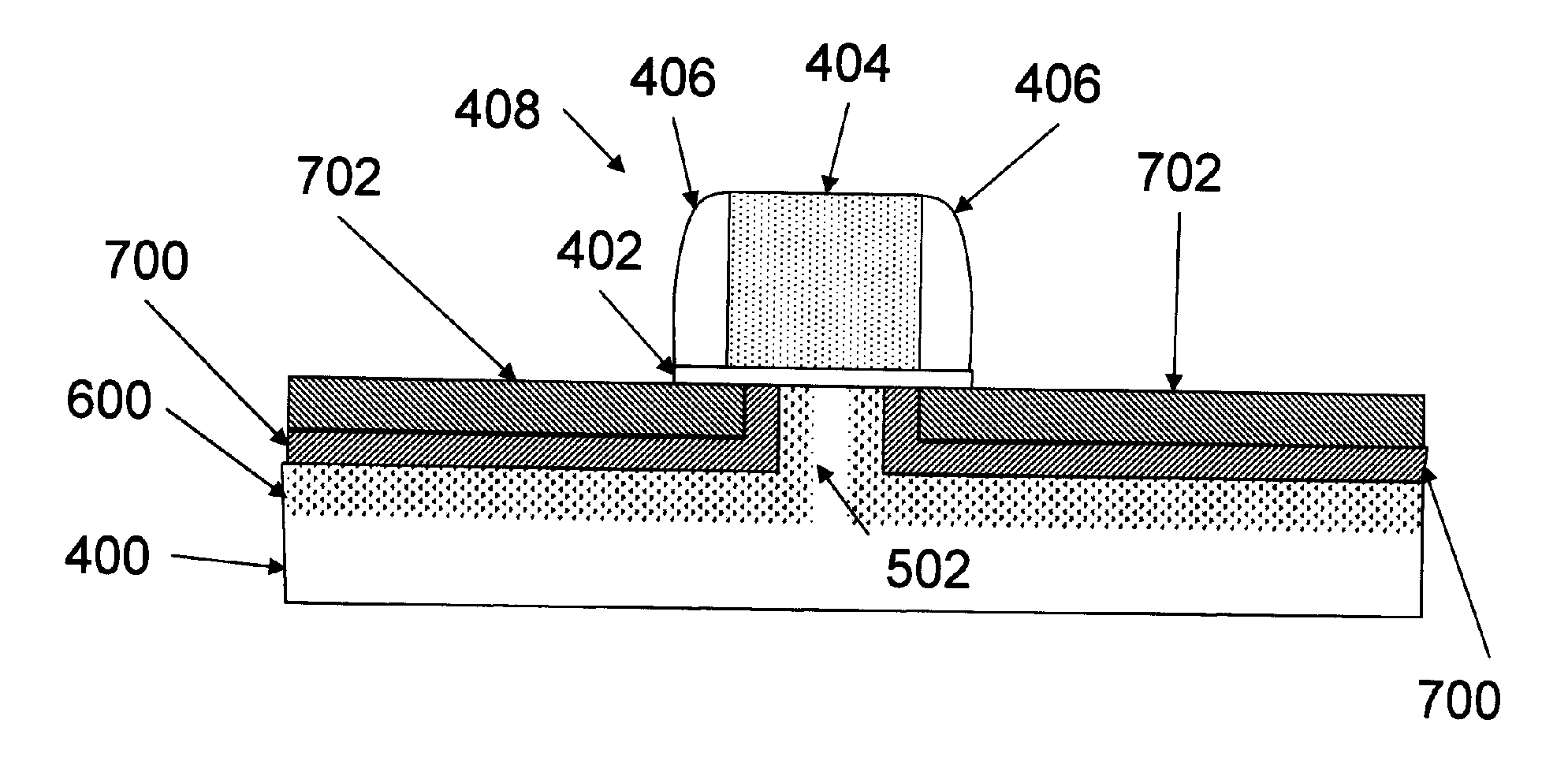
[0021] As mentioned above, the invention presents a beneficial method of forming a field effect transistor that creates shallower and sharper junctions, while maximizing dopant activation in processes that are consistent w...
PUM
 Abstract
Description
Claims
Application Information