Reliability circuit for applying an AC stress signal or DC measurement to a transistor device

a transistor device and reliability technology, applied in the field of reliability circuits, can solve the problems of difficult to apply an ac stress signal to a mos transistor in a bench system, difficult to be sure that the stress and measurement and setup is precise, and difficult to apply an accurate ac bias signal to a device under tes

Inactive Publication Date: 2006-04-13
AVAGO TECH INT SALES PTE LTD
View PDF7 Cites 17 Cited by
  • Summary
  • Abstract
  • Description
  • Claims
  • Application Information

AI Technical Summary

Benefits of technology

[0008] Another embodiment of the present invention is directed to an integrated circuit, which includes a transistor device under test, an AC drive circuit, an AC bias circuit, DC measurement pins and a DC bias circuit. The AC drive circuit generates an AC drive signal. The AC bias circuit couples to the transistor device such that the device is an element within an inverter, and drives the transistor device in response to the AC drive signal. The DC bias circuit biases the transistor device under DC bias conditions. The DC measurement pins are coupled to the DC bias circuit for providing inputs to control the DC bias conditions and for providing DC measurement outputs. A switch circuit selectively couples the transistor device to the AC bias circuit in an AC stress mode and to the DC bias circuit in a DC measurement mode.

Problems solved by technology

However, it is difficult to apply an AC stress signal to a MOS transistor in a bench system because the AC stress signal is modified by the parasitic inductance and capacitance of the test tool and the cables in the signal path that apply the AC stress signal to the device under test.
It is difficult to be sure that the stress and measurement and setup is precise and that the signal applied to device under test is what is expected or desired.
Again, it is very difficult to apply an accurate AC bias signal to a device under test, particularly during a burn-in test.
Another difficulty that arises with reliability test circuits is that the induced AC voltage or temperature stress that is applied to the device under test is also applied to the surrounding circuitry that delivers the drive signals and stress to the device.
This further complicates the extraction of accurate model parameters and measurements and complicates the failure analysis of failing components.

Method used


Image

  • Reliability circuit for applying an AC stress signal or DC measurement to a transistor device
  • Reliability circuit for applying an AC stress signal or DC measurement to a transistor device
  • Reliability circuit for applying an AC stress signal or DC measurement to a transistor device

Examples


Embodiment Construction

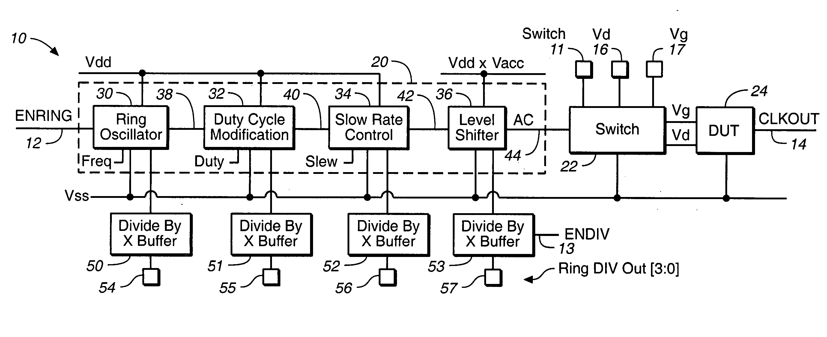
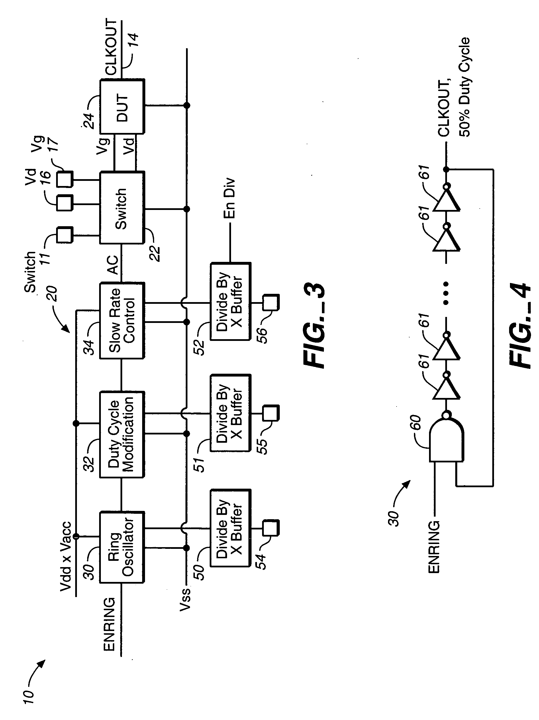
[0028] One embodiment of the present invention implements the AC drive circuit on the same integrated circuit as the device under test is fabricated. The AC drive circuit has the ability to vary the frequency, duty cycle, slew rate and amplitude of the AC drive signal, thereby enabling the circuit to monitor degradation mechanisms for all varieties of NMOS and PMOS devices integrated in CMOS technologies.

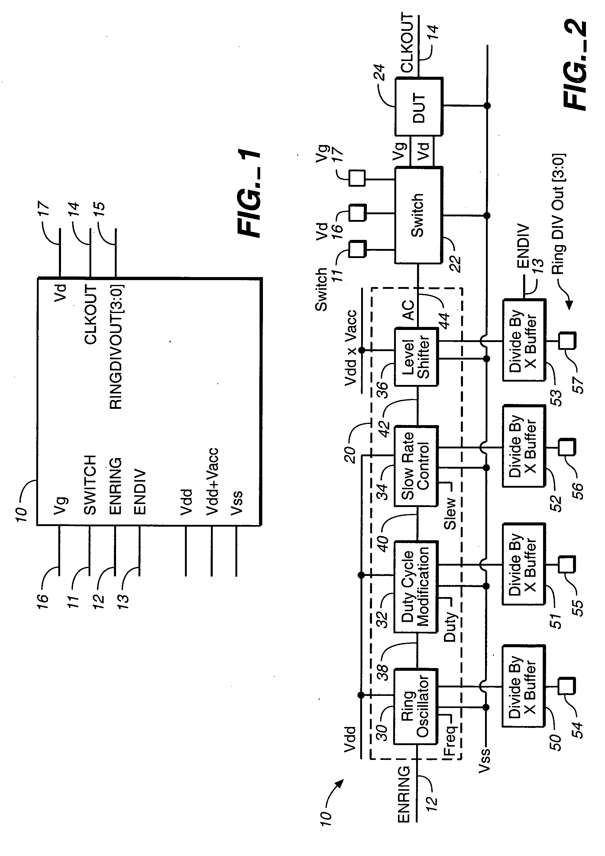
[0029]FIG. 1 is a diagram illustrating a semiconductor integrated circuit 10 on which a metal oxide semiconductor (MOS) device is fabricated for reliability testing purposes. As described in more detail below and shown in the remaining figures, integrated circuit 10 includes one or more reliability test circuits for testing one or more transistor devices that are fabricated on integrated circuit 10. The device under test can include one or more N-channel devices and / or one or more P-channel devices. Although embodiments of the present invention are discussed with respect to MOS dev...


PUM


Abstract

An integrated circuit is provided, which includes a transistor device under test, an AC drive circuit, an AC bias circuit and a DC bias circuit. The AC drive circuit generates an AC drive signal. The AC bias circuit biases the transistor device under AC bias conditions in response to the AC drive signal. The DC bias circuit biases the transistor device under DC bias conditions. A switch circuit selectively couples the transistor device to the AC bias circuit in an AC stress mode and to the DC bias circuit in a DC measurement mode.

Description

FIELD OF THE INVENTION [0001] The present invention relates to semiconductor integrated circuits and, more particularly to a reliability circuit for applying an AC stress signal to a transistor device under test and then applying a DC measurement to the device. BACKGROUND OF THE INVENTION [0002] The characteristics of semiconductor devices are often modeled in order to evaluate their reliability under different operating conditions. Typically, these tests are performed as a bench test in which an external device is coupled to an integrated circuit under test. The external device exercises one or more transistor devices on the integrated circuit with a time-varying AC stress signal. These bench tests often use a waveform generator for supplying the AC stress signal. After the transistor devices have been stressed at a predetermined temperature for a predetermined period of time, a different external device measures the resulting operating characteristics of the transistor device or d...

Claims


Application Information

Patent Timeline
Patent Type & Authority Applications(United States)
IPC IPC(8): G01R31/26
CPCG01R31/2642G01R31/2856H01L22/34H01L2924/0002H01L2924/00
Inventor WALKER, JOHN D.PARK, SANGJUNESCHULTZ, RICHARD T.
Owner AVAGO TECH INT SALES PTE LTD
Why Eureka
Try Eureka