Semiconductor device and method of manufacturing the same

a semiconductor and liquid crystal display technology, applied in the direction of optics, instruments, electrical equipment, etc., can solve the problems of disturbing the display picture, affecting the efficiency of light utility, and affecting the effect of brightness, etc., and achieve excellent effects

Inactive Publication Date: 2006-04-13
SEMICON ENERGY LAB CO LTD
View PDF28 Cites 16 Cited by
  • Summary
  • Abstract
  • Description
  • Claims
  • Application Information

AI Technical Summary

Benefits of technology

[0016] An object of the present invention is therefore to solve the above-mentioned problems and to provide means for forming an extremely fine active matrix type display device by a simple process.
[0023] If the flattening is made within 20% of the thickness of the electrode, it is possible to suppress the influence of unevenness to the thickness of the liquid crystal layer. Especially, in the case of a reflection type liquid crystal panel, since poor display due to the unevenness of the thickness of the liquid crystal layer becomes tangible, it is effective to use the present invention disclosed in the present specification.
[0025] Although it is preferable that the flattening is restricted within 20% of the thickness of the pixel electrode, in practical viewpoint, it is effective even if the flattening is restricted within 50% of the pixel electrode.
[0026] As to the degree of flatness, assuming that the surface state as shown in FIG. 13 is obtained, it is appropriate to realize such flatness that the value of θ is not larger than 15°. By doing so, it is possible to effectively use the light reflected by a reflecting pixel electrode formed thereon in optical modulation. Of course, in the state shown in FIG. 13, it is important to make the value of “c” not larger than 20 to 60 nm.
[0028] If these limiting conditions are combined with other parameters, they become more effective. That is, if the flatness is secured so as to satisfy the limiting conditions of these parameters or conditions regulated by the combination of limiting conditions of the respective parameters, more excellent effects of the present invention can be obtained.

Problems solved by technology

Poor orientation of a liquid crystal material occurs at such a difference in level, so that a displayed picture is disturbed.
Besides, diffused reflection of incident light at the portion of the difference in level causes the contrast to lower or the efficiency of utility of light to lower.
Such a difference in level also causes the foregoing problems.
However, in the case where the black mask is provided at the TFT side substrate, there arises various problems such as increase of patterning steps, increase of parasitic capacitance, and lowering of an aperture factor.

Method used


Image

  • Semiconductor device and method of manufacturing the same
  • Semiconductor device and method of manufacturing the same
  • Semiconductor device and method of manufacturing the same

Examples


embodiment 1

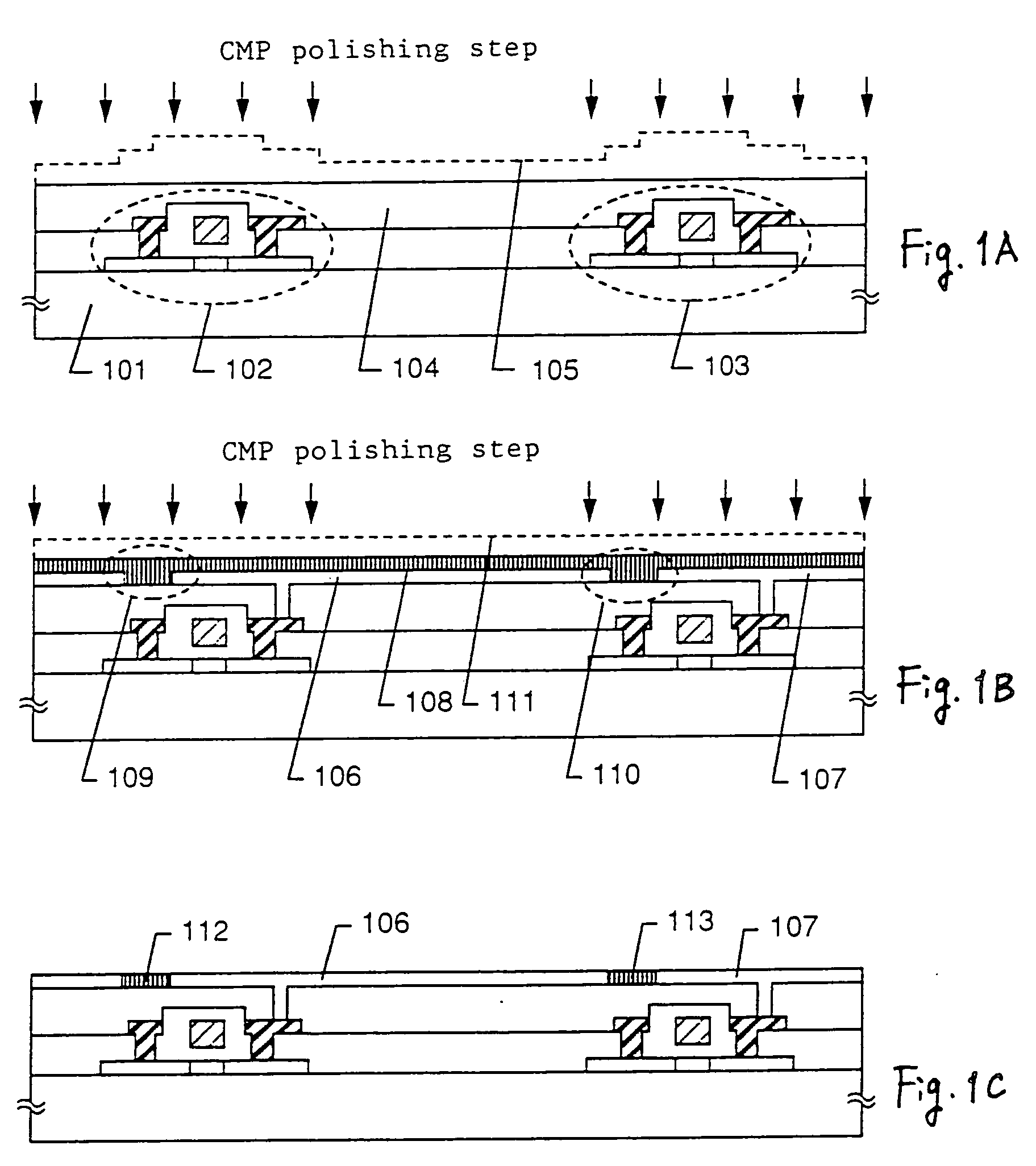
[0060] In this embodiment, an example of steps of manufacturing a pixel matrix circuit of a reflection type LCD using the present invention will be described with reference to FIGS. 3 and 4. Since the present invention relates to a technique for flattening a pixel, a TFT structure itself is not limited to this embodiment.

[0061] First, a substrate 301 having an insulating surface is prepared. In this embodiment, a silicon oxide film as an under layer is formed on the glass substrate. Active layers 302 to 304 made of crystalline silicon films are formed on the substrate 301. In this embodiment, although only three TFTs are shown, actually a million TFTs or more are formed in a pixel matrix circuit.

[0062] In this embodiment, an amorphous silicon film is thermally crystallized to obtain a crystalline silicon film. The crystalline silicon film is patterned by a normal photolithography step to obtain the active layers 302 to 304. In this embodiment, a catalytic element (nickel) for prom...

embodiment 2

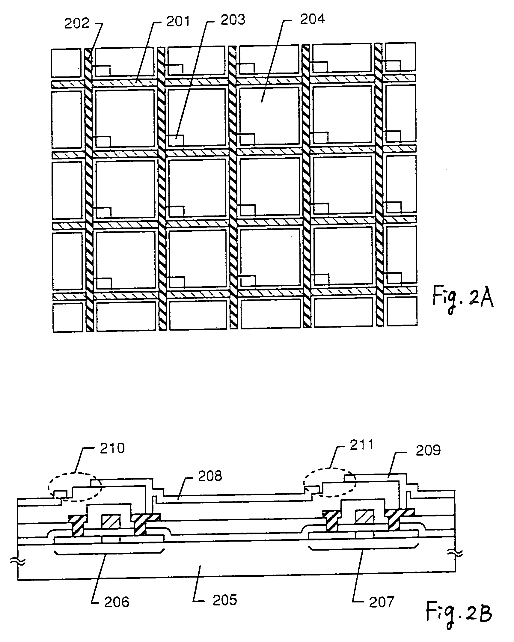
[0088] In this embodiment, an example of steps of manufacturing a pixel matrix circuit of a transmission type LCD by using the present invention will be described with reference to FIGS. 5A to 5C. Since the steps are the same as those of the reflection type LCD shown in the Embodiment 1 partway, only different points will be described here.

[0089] After the first CMP polishing step as shown in FIG. 3D is ended, pixel electrodes 501 and 502 shown in FIG. 5A are formed. In this embodiment, as the material for the pixel electrodes 501 and 502, transparent conductive films (ITO, SnO2, etc.) are used. At this time, the pixel electrodes 501 and 502 are formed so that they do not overlap with the TFTs.

[0090] Next, an insulating layer 503 covering the pixel electrodes 501 and 502 is formed. In this embodiment, for the insulating layer 503, polyimide with a dispersed black pigment or the like is used. In the case of the transmission type, since the active layer of the TFT is also required t...

embodiment 3

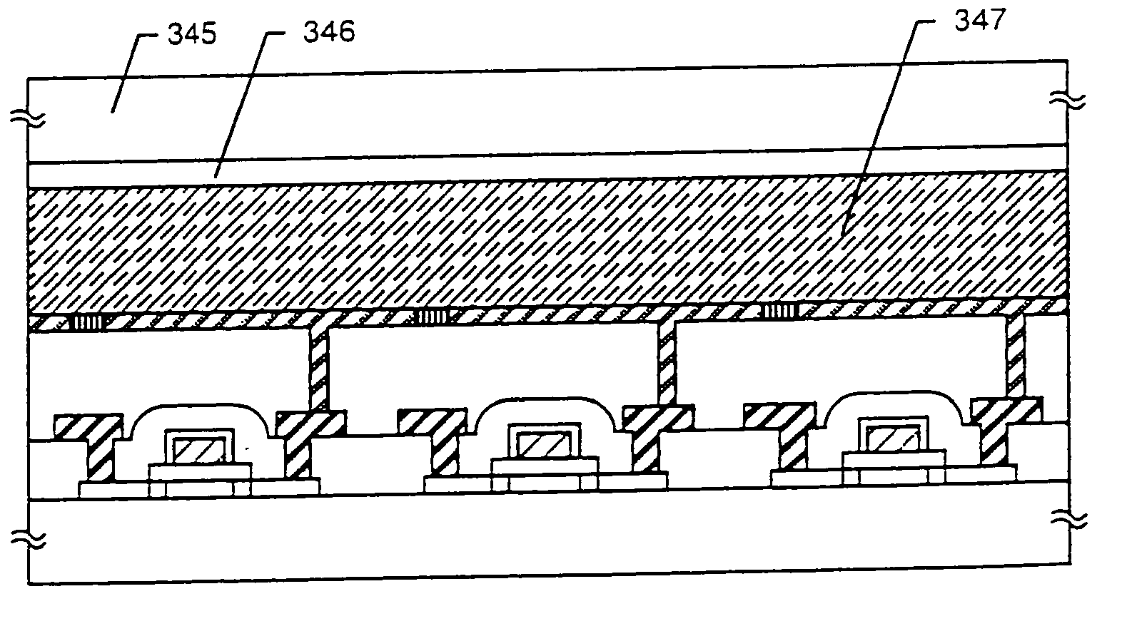
[0096] In the manufacturing steps of the embodiment 1, only the second interlayer insulating film 337 and the embedded insulating layer 341 are flattened. However, in the present invention, it is also possible to make a flattening step to the first interlayer insulating layer 330.

[0097] In the case where an interlayer insulating film is formed of a lamination structure, it is also possible to make a flattening step for every formation of the respective layers.

[0098] In the present invention, before pixel electrodes are formed, sufficient flatness is secured, and further, the gaps between the pixel electrodes are filled with the embedded insulating layers to improve the flatness of the surfaces of the pixel electrodes. Thus, there is no problem even if the number of flattening steps is large, rather it is preferable.


PUM

PropertyMeasurementUnit
sizeaaaaaaaaaa
thicknessaaaaaaaaaa
flatnessaaaaaaaaaa

Abstract

To provide an active matrix type liquid crystal display device having fine display performance, an interlayer insulating film 104 covering TFTs 102, 103 formed on a substrate 101 is first flattened by mechanical polishing typified by a CMP. Then pixel electrodes 106, 107 are formed thereon, and further, an insulating layer 108 covering the pixel electrodes is formed. And then, the insulating layer 108 is flattened by second mechanical polishing so that the surfaces of the pixel electrodes and the surface of the insulating layers 112, 113 form the same plane. By this, a difference in level disappears, and it is possible to prevent lowering of contrast or the like due to poor orientation of a liquid crystal material, diffused reflection of light, and the like.

Description

BACKGROUND OF THE INVENTION [0001] 1. Field of the Invention [0002] The present invention relates to a method of manufacturing a liquid crystal display device (LCD), and particularly to a method of manufacturing an active matrix type liquid crystal display device using a semiconductor thin film (hereinafter referred to as an AM-LCD). The present invention can be applied to an electrooptical device equipped with such a display device. [0003] Incidentally, in the present specification, the term “semiconductor device” indicates all devices which function by using a semiconductor. Thus, the foregoing display device and the electrooptical device are included in the category of the semiconductor device. However, in the present specification, for facilitation of the distinction, terms such as a display device and an electrooptical device are selectively used. [0004] 2. Description of the Related Art [0005] In recent years, a projector or the like using the AM-LCD as a projection type displ...

Claims


Application Information

Patent Timeline
Patent Type & Authority Applications(United States)
IPC IPC(8): G02F1/13G02F1/136G02F1/1333G02F1/1362G02F1/1368H01L21/336H01L29/786
CPCG02F1/133553G02F1/1362G02F1/136209G02F1/136227G02F1/136277G02F2001/133357G02F2201/48G02F1/133357
Inventor HIRAKATA, YOSHIHARUYAMAZAKI, SHUNPEI
Owner SEMICON ENERGY LAB CO LTD
Why Eureka
Try Eureka