Method and apparatus for placing conductive balls

a technology of placing apparatus and conductive balls, which is applied in the direction of packaging, printed circuit assembling, lithographic masks, etc., can solve the problems of improper placement of conductive balls, deformation of conductive balls, and particularly obvious problems, and achieve the effect of improving the placement ratio of conductive balls

Inactive Publication Date: 2006-04-27
HITACHI METALS LTD
View PDF6 Cites 27 Cited by
  • Summary
  • Abstract
  • Description
  • Claims
  • Application Information

AI Technical Summary

Benefits of technology

[0028] The object of the present invention is to provide an improved placing method and placing apparatus for placing conductive balls in a predetermined pattern onto a base unit where the conductive balls are arranged thereon. One object of the present invention is to provide a placing method and...

Problems solved by technology

However, the conductive balls might be deformed due to the suction force of the suction head.
Therefore, an improper placement of the conductive balls may occur.
This problem will be particularly obvious as the diameter of the conductive balls becomes smaller and smaller.
However, problems occur when the diameter of the conductive balls becomes smaller.
However, if the conductive balls are small in diameter and mass, the conductive balls that are loaded into the positioning openings fall with small energy to impact with the flux.
Therefore, as the conductive balls are adhered at the positioning openings by the suction force, conductive balls are not properly placed on the electrodes.
In addition, as ...

Method used


Image

  • Method and apparatus for placing conductive balls
  • Method and apparatus for placing conductive balls
  • Method and apparatus for placing conductive balls

Examples


first embodiment

1. FIRST EMBODIMENT

[0073] One example of the present invention according to the first embodiment is described with reference to FIGS. 1 to 14.

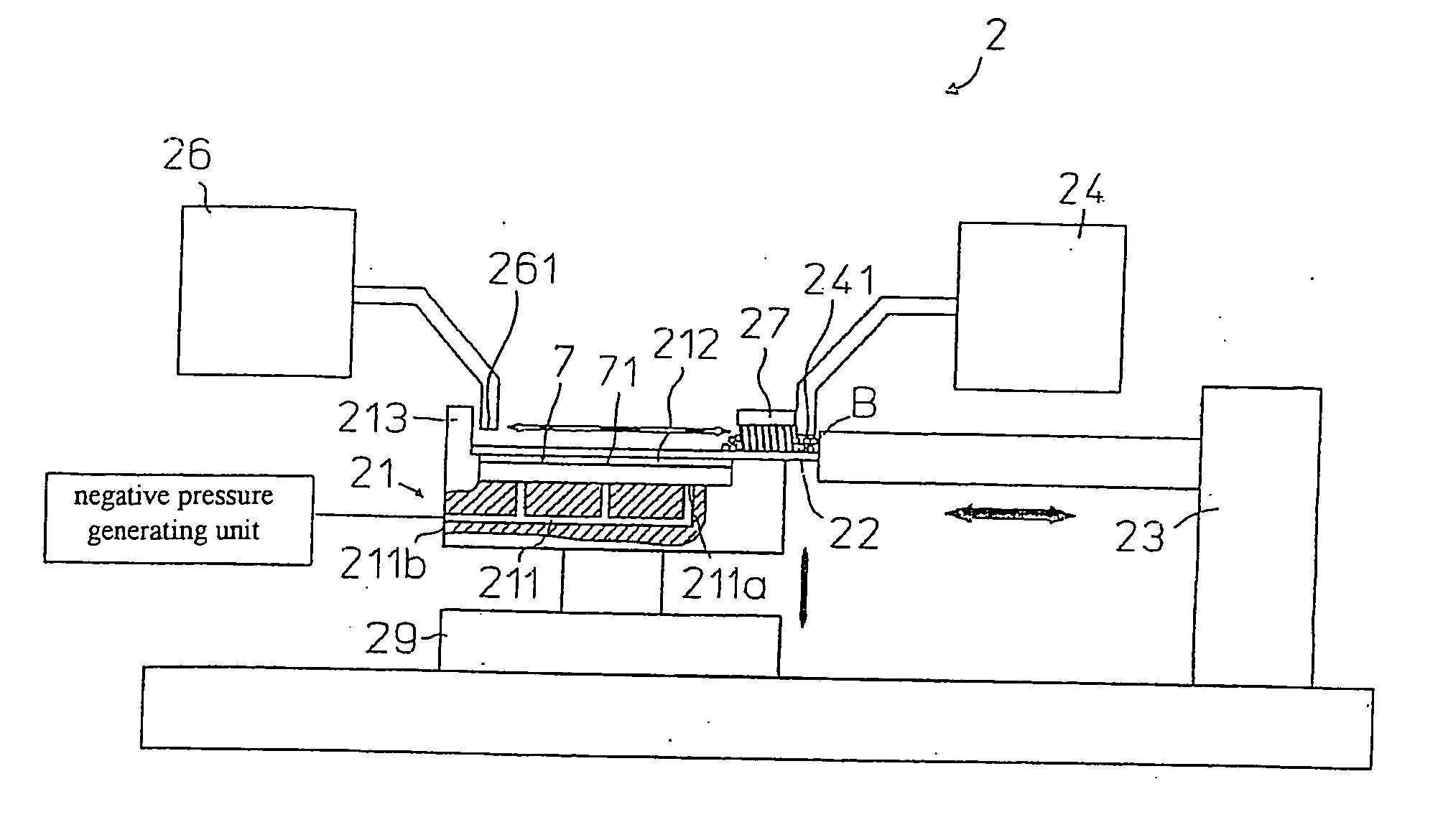
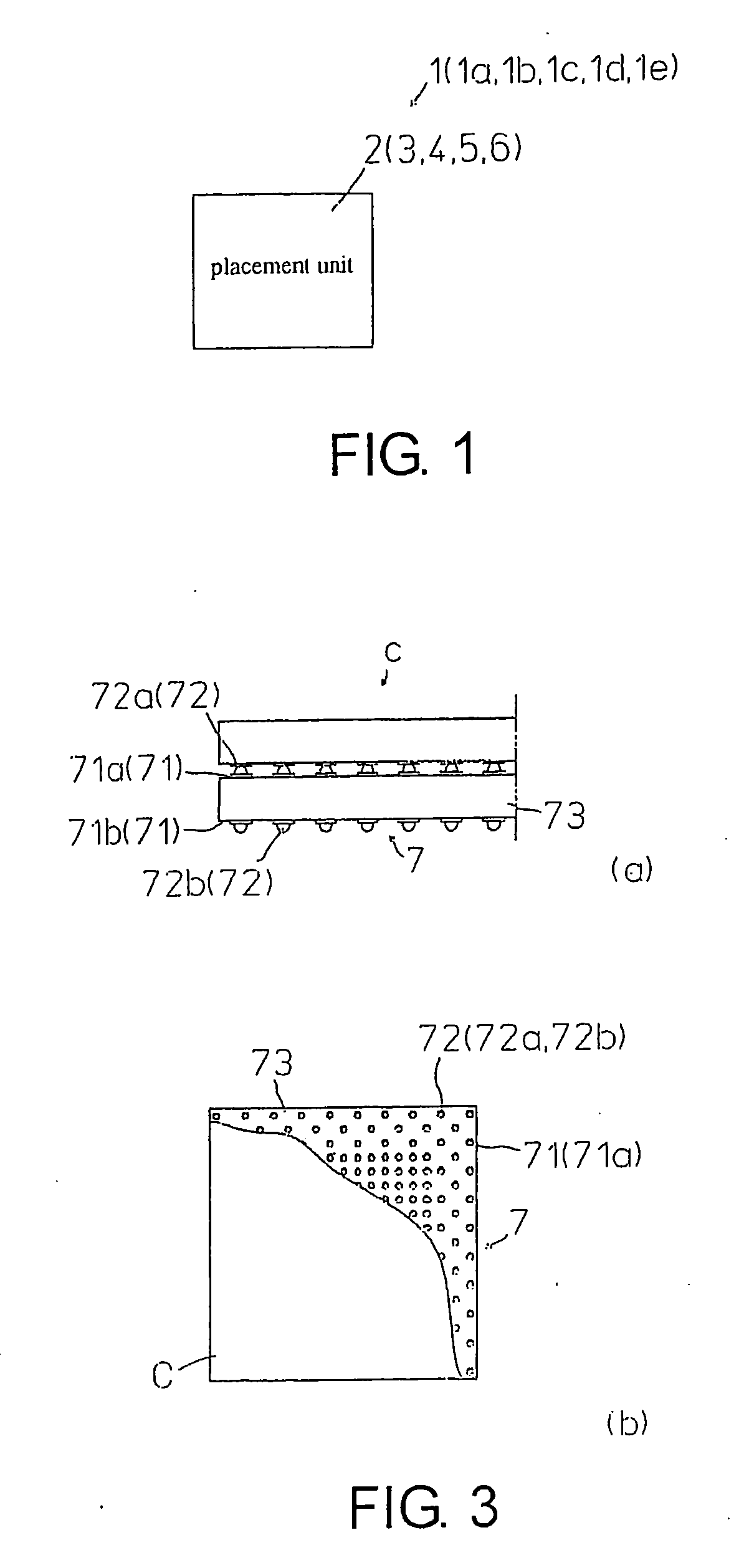
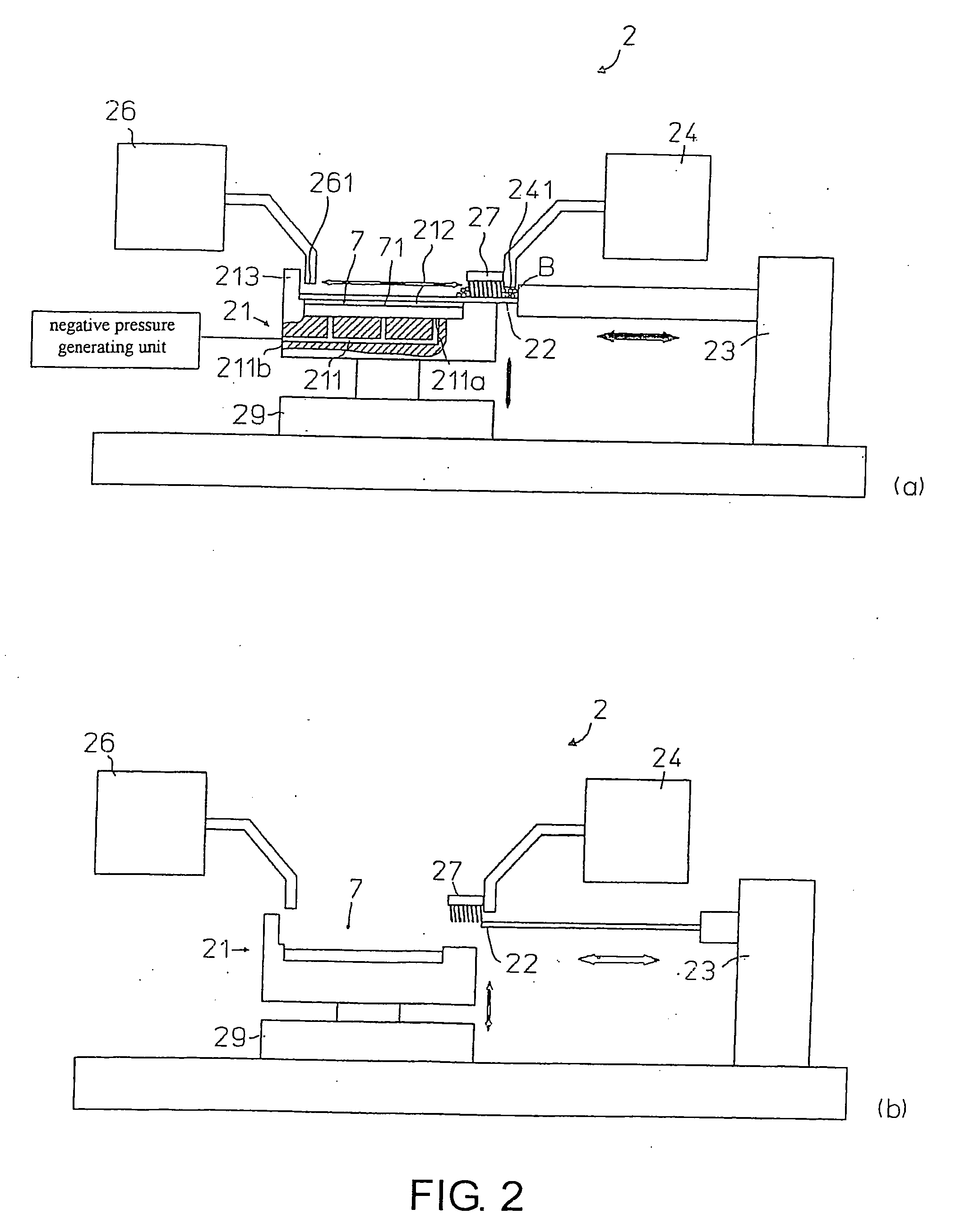
[0074] As shown in FIG. 1, the placement device 1a of the first embodiment comprises a placement unit 2 for arranging and placing solder balls onto a substrate, i.e., a base unit.

[0075] As shown in FIG. 3, connection bumps 72b (72), connected to an external device such as a motherboard, are protruded from one surface (lower surface) of the substrate 7 in an area array pattern, and connection bumps 72a (72), connected to a semiconductor element 8, are protruded from another surface (upper surface) of the substrate 7 in an area array pattern. The semiconductor element 8 is bonded to the upper surface of the substrate 8 by a flip-chip bonding method, and a package is thus formed.

[0076] The substrate 7 has a thin-plate base substance 71, pot-shaped electrodes 71a (71) where the aforementioned connection bumps 72a are protruded form the upper su...

second embodiment

2. THE SECOND EMBODIMENT

[0120] The second embodiment of the present invention is described with reference to FIGS. 15 to 17. Additionally, in the drawings, constituents substantially the same as the placement device 1a of the first embodiment are labeled with the same symbols, and their structure and detail operations are omitted (following descriptions for other embodiments are the same).

[0121] As shown in FIG. 1, the placement device 1b of the second embodiment comprises a placement unit 3 for arranging and placing the solder balls onto the substrate, i.e., the base unit.

[0122] As shown in FIG. 15, the placement unit 3 of the second embodiment and the placement unit 2 of the first embodiment are basically the same structure. The placement unit 3 comprises a mask 22, a transfer device 27′, a holder 31, a holder raising unit 29, a mask horizontal moving unit 23, a ball supplying unit 24 and a ball removing unit 26. The mask 22 is an arrangement member for arranging the solder ball...

third embodiment

3. THIRD EMBODIMENT

[0139] The third embodiment of the present invention is described with reference to FIG. 1 and FIGS. 18-20.

[0140] As shown in FIG. 1, the placement device 1c has a placement unit 4 for aligning and placing the solder balls onto the substrate 7, i.e., the base unit.

[0141] As shown in FIG. 18, the placement unit 4 of the third embodiment and the placement 2 of the first embodiment are basically the same structure. The placement unit 4 comprises a mask 22′, a transfer device 27, a holder 41, a holder raising unit 29, a mask horizontal moving unit 23, a ball supplying unit 24 and a ball removing unit 26. The mask 22′ is an arrangement member for arranging the solder balls B onto the electrodes 71 of the substrate 7. The transfer device 27 is horizontally moved to the upper surface of the mask 22′ positioned on the substrate 7 by a moving unit (not shown), so as to transfer the solder balls B. To be suited for automation, the holder 41 keeps the position of the subst...


PUM

PropertyMeasurementUnit
Timeaaaaaaaaaa
Timeaaaaaaaaaa
Angleaaaaaaaaaa

Abstract

Improved placing method and apparatus are provided for placing conductive balls in a predetermined pattern onto one surface of a base unit. An arrangement member is provided to have one surface, another surface opposite to the one surface of the arrangement member and positioning openings. The positioning openings are arranged corresponding to the pattern so that the balls are inserted therein. The another surface of the arrangement member is opposite to the one surface of the base unit. The arrangement member has two or more line members whose core axes are substantially aligned. The transfer device is arranged so that the line members are substantially in a horizontal position to contact with the balls, and then the transfer device is horizontally moved with respect to the one surface of the arrangement member. Then, the balls are placed on the one surface of the base unit through the positioning openings.

Description

BACKGROUND OF THE INVENTION [0001] 1. Field of the Invention [0002] This invention relates a placing method and a placing apparatus for placing balls with conductivity that are arranged in a predetermined pattern on a base unit, such as electronic parts or parts used for fabricating electronic parts etc. [0003] 2. Background Technology [0004] Electronic parts like semiconductor devices, substrates or packages thereof with protruded connection bumps of area array type, such as BGA (Ball Grid Allay) type and FC (Frip-Chip) type, etc., can be examples of the base unit. On the base unit, balls with conductivity (conductive balls, hereinafter) are placed in a predetermined pattern. [0005] In recent years, as the portable machines and notebook computers progress in the direction of high speed, high performance, lightweight, small-size and thin shape, the performances of a large-dimension device and multiple terminals are required for the built-in electronic components. In responding to su...

Claims


Application Information

Patent Timeline
IPC IPC(8): B31B1/60B23K3/06H01L21/48H01L21/60H05K3/34
CPCB23K3/0623Y10T156/10H01L24/11H01L2224/13099H01L2924/01002H01L2924/01013H01L2924/01022H01L2924/01029H01L2924/01033H01L2924/01042H01L2924/01047H01L2924/01058H01L2924/01074H01L2924/01078H01L2924/01079H01L2924/01082H01L2924/3011H01L2924/3025H05K3/3478H05K2203/041H05K2203/0485H05K2203/0557H05K2203/104H01L2224/11005H01L24/742H01L2224/11003H01L2224/11334H01L2924/01005H01L2924/01006H01L2924/014Y10T29/49204H01L21/4853H01L2224/05568H01L2224/05573H01L2224/0615H01L2924/00014H01L2924/12042H01L2924/00H01L2224/05599H05K3/34
Inventor ITOH, MOTOYUKIOCHIAI, MASANORIKAZUI, SHINICHI
Owner HITACHI METALS LTD
Why Eureka
Try Eureka