Nonplanar device with thinned lower body portion and method of fabrication

Inactive Publication Date: 2006-04-27
INTEL CORP
View PDF99 Cites 106 Cited by
  • Summary
  • Abstract
  • Description
  • Claims
  • Application Information

AI Technical Summary

Problems solved by technology

Unfortunately, the fourth side, the bottom part of the channel is isolated from the g

Method used


Image

  • Nonplanar device with thinned lower body portion and method of fabrication
  • Nonplanar device with thinned lower body portion and method of fabrication
  • Nonplanar device with thinned lower body portion and method of fabrication

Examples


Embodiment Construction

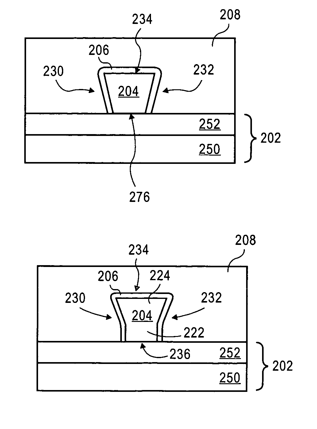
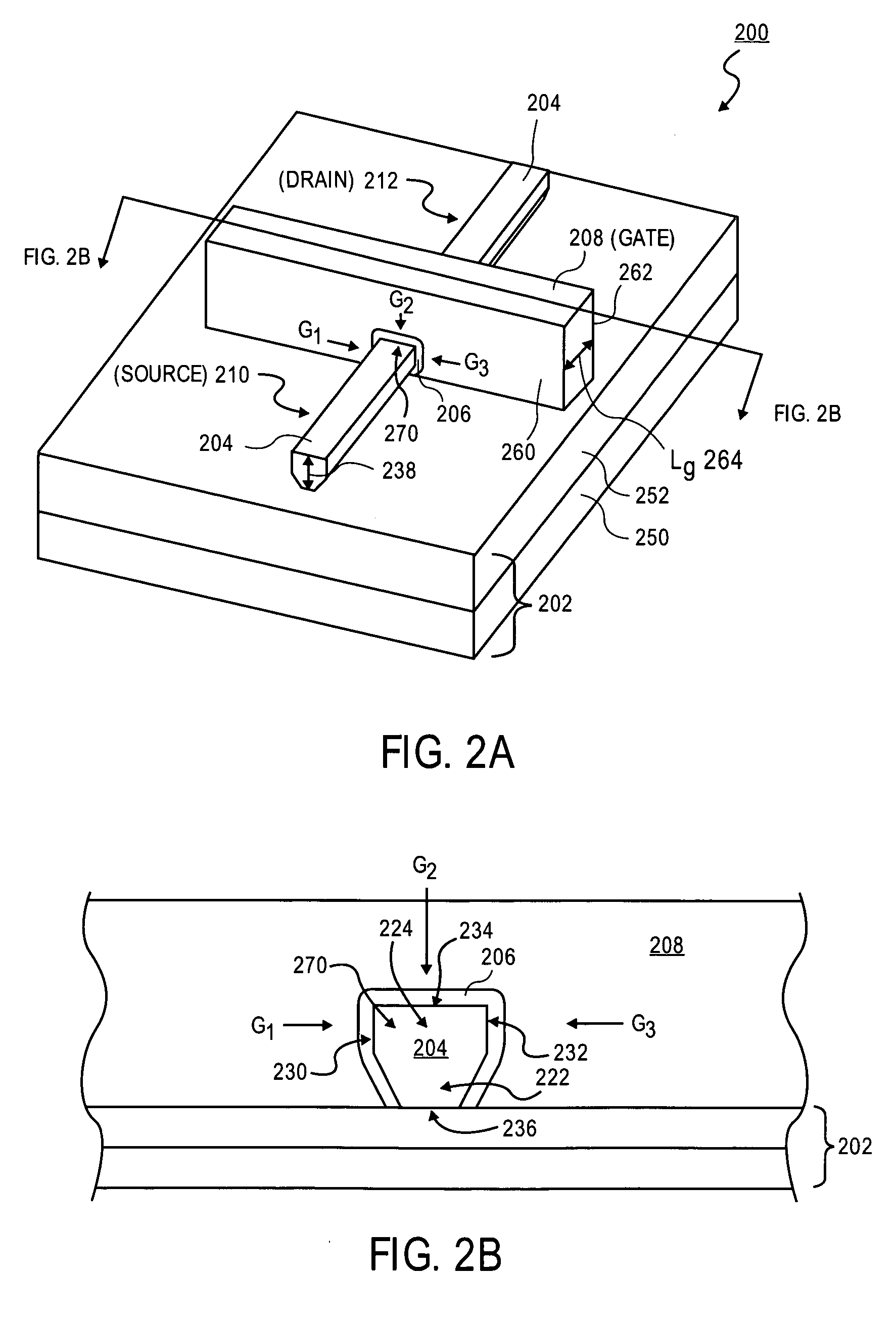
[0012] The present invention is a novel nonplanar device with a thinned lower body portion and a method of fabrication. In the following description, numerous specific details are set forth in order to provide a thorough understanding of the present invention. In other instances, well known semiconductor processes and manufacturing techniques have not been described in particular detail in order to not unnecessarily obscure the present invention.

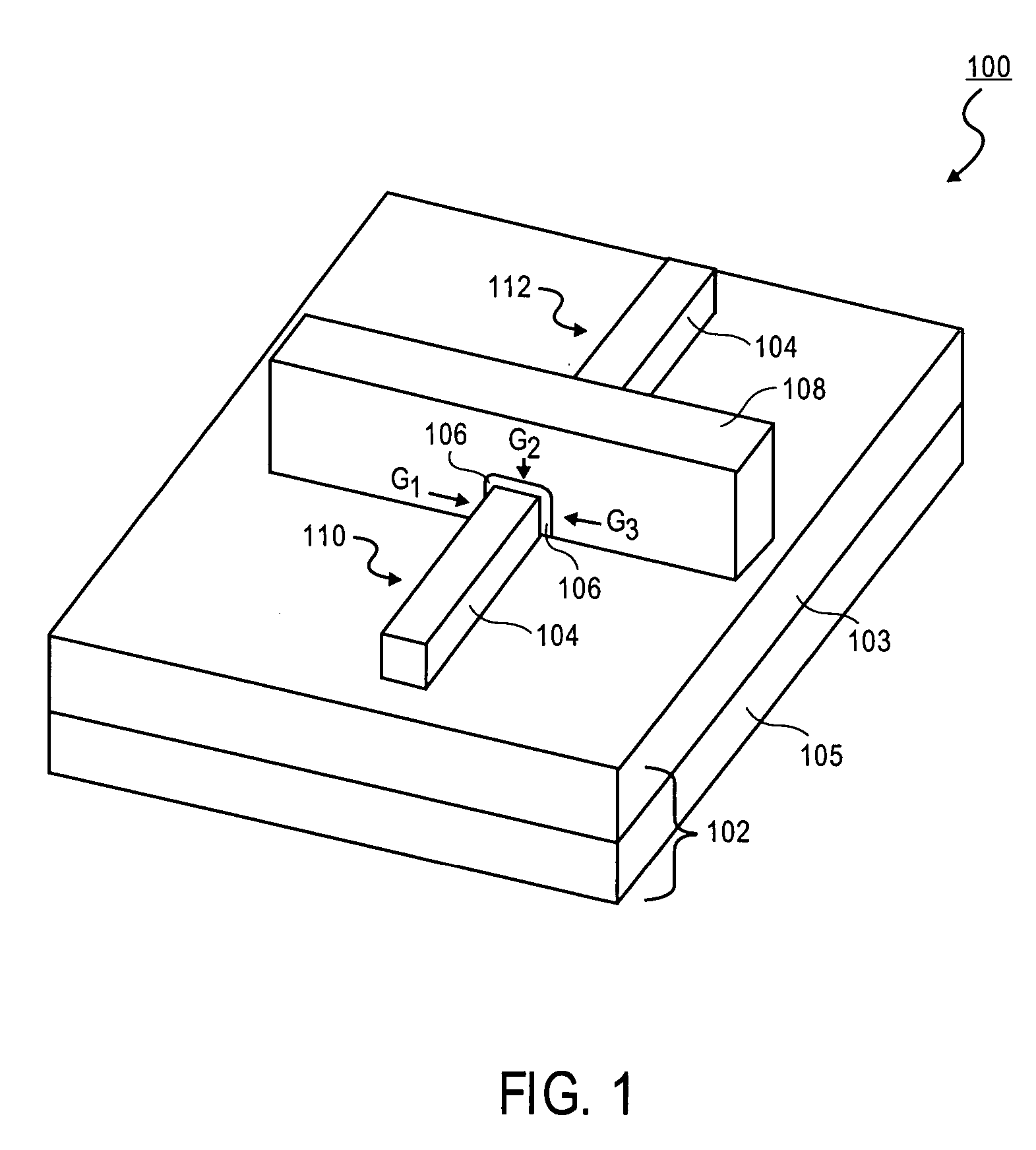
[0013] Embodiments of the present invention include a nonplanar or tri-gate transistor having a semiconductor body which is wrapped around on three sides by a gate dielectric layer and a gate electrode. In embodiments of the present invention, the bottom portion of the semiconductor body is made thinner than the top portion of the semiconductor body. Making the bottom portion of the semiconductor body thinner than the top portion increases the gate control over the bottom portion of the body resulting in better short channel effects. In an ...


PUM


Abstract

A nonplanar semiconductor device having a semiconductor body formed on an insulating layer of a substrate. The semiconductor body has a top surface opposite a bottom surface formed on the insulating layer and a pair of laterally opposite sidewalls wherein the distance between the laterally opposite sidewalls at the top surface is greater than at the bottom surface. A gate dielectric layer is formed on the top surface of the semiconductor body and on the sidewalls of the semiconductor body. A gate electrode is formed on the gate dielectric layer on the top surface and sidewalls of the semiconductor body. A pair of source/drain regions are formed in the semiconductor body on opposite sides of the gate electrode.

Description

BACKGROUND OF THE INVENTION [0001] 1. Field of the Invention [0002] The present invention relates to the field of semiconductor devices and more particularly to a nonplanar tri-gate transistor having a thinned lower body portion and method of fabrication. [0003] 2. Discussion of Related Art [0004] In order to increase the performance of modern integrated circuits, such as microprocessors, silicon on insulator (SOI) transistors have been proposed. Silicon on insulator (SOI) transistors have an advantage in that they can be operated in a fully depleted manner. Fully depleted transistors have an advantage of ideal subthreshold gradients for optimized ON current / OFF current ratios. [0005] An example of a proposed SOI transistor which can be operated in a fully depleted manner is a tri-gate transistor 100, such as illustrated in FIG. 1. Tri-gate transistor 100 includes a silicon body 104 formed on an insulating substrate 102 having a buried oxide layer 103 formed on a monocrystalline sil...

Claims


Application Information

Patent Timeline
IPC IPC(8): H01L27/12H01L27/01H01L31/0392
CPCH01L29/42384H01L29/66818H01L29/7853H01L29/785Y10S438/978H01L21/823431H01L21/845H01L27/0886H01L27/1211H01L29/66795H01L29/7854H01L29/7856H01L2924/13067
Inventor SHAH, UDAYDOYLE, BRIANBRASK, JUSTIN K.CHAU, ROBERT S.LETSON, THOMAS A.
Owner INTEL CORP
Why Eureka
Try Eureka