Semiconductor device and manufacturing method thereof

a semiconductor and semiconductor technology, applied in the direction of semiconductor devices, basic electric elements, electrical equipment, etc., can solve the problems of reducing the reliability of elements, and achieve the effects of reducing the stress resulting from the trench isolation formed in the semiconductor substrate, reducing the cost of manufacturing, and improving the heat release through the trench isolation region

Inactive Publication Date: 2006-04-27
PANASONIC CORP
View PDF5 Cites 51 Cited by
  • Summary
  • Abstract
  • Description
  • Claims
  • Application Information

AI Technical Summary

Benefits of technology

[0018] According to the semiconductor device of the second aspect of the invention, stress resulting from trench isolation formed in a semiconductor substrate of silicon or in the semiconductor layer of silicon can be easily reduced without precisely controlling the composition of the trench filler. Moreover, since the insulating metal nitride has higher thermal conductance than that of silicon oxide, heat release through the trench isolation region is improved. Such reduced stress and improved heat conduction of the trench isolation region improve reliability of the semiconductor device.
[0019] Note that, unlike the semiconductor device of the first aspect of the invention, only a part of the trench is filled with the insulating metal nitride in the semiconductor device of the second aspect of the invention. Therefore, reduction in stress and improvement in heat conduction in the trench isolation region are less than those in the semiconductor device of the first aspect of the invention. However, filling the remaining part of the trench with silicon oxide or the like facilitates planarization of the upper part of the trench isolation region because silicon oxide is softer than nitrides. Moreover, since silicon oxide is highly compatible with a semiconductor process, unexpected defects are less likely to be generated.

Problems solved by technology

As well known in the art, increased power consumption per unit area raises the temperature of elements, resulting in reduced reliability of the elements.

Method used


Image

  • Semiconductor device and manufacturing method thereof
  • Semiconductor device and manufacturing method thereof
  • Semiconductor device and manufacturing method thereof

Examples


first embodiment

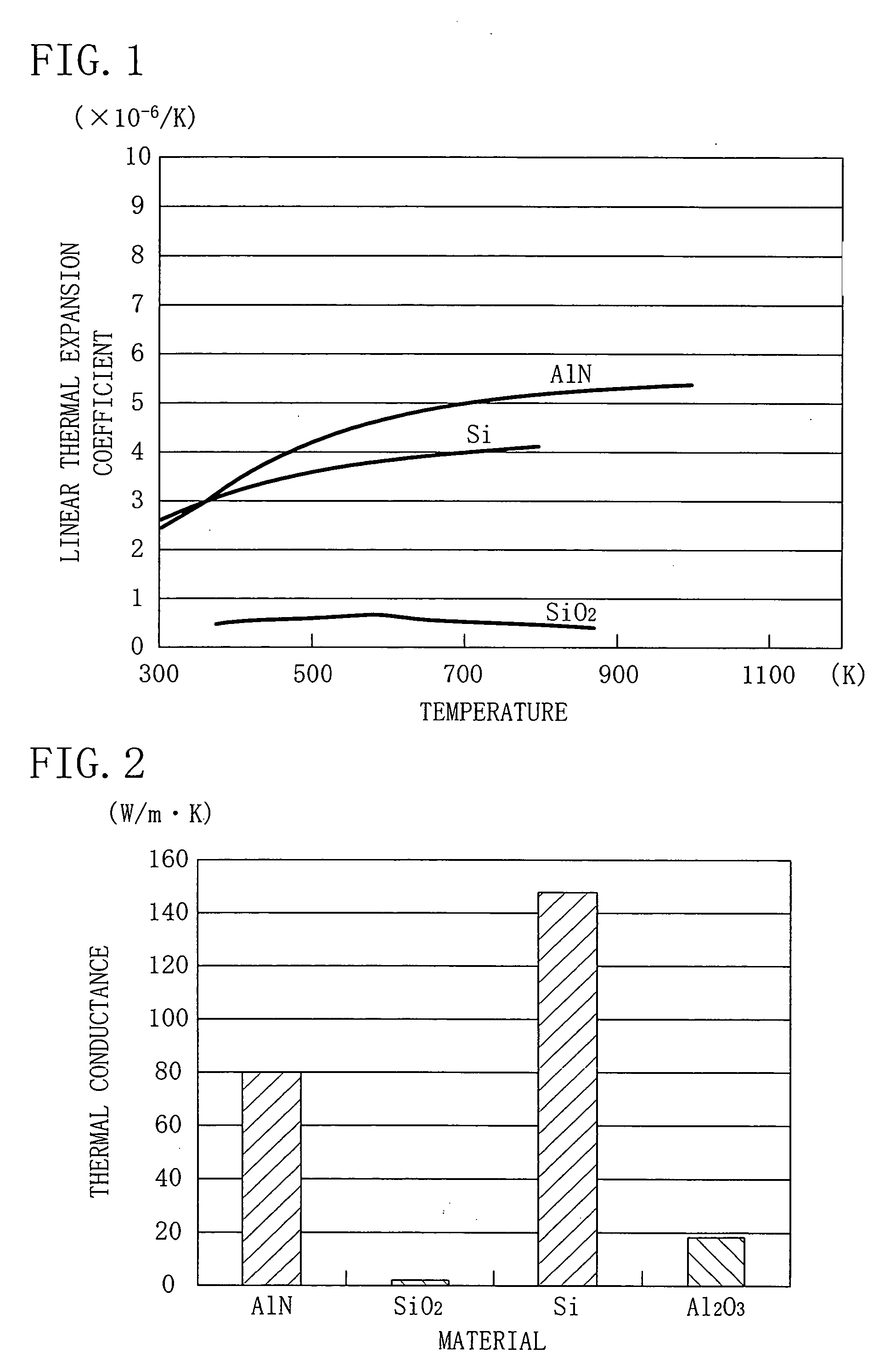
[0053] Hereinafter, a semiconductor device and a manufacturing method thereof according to a first embodiment of the present invention will be described with reference to the drawings.

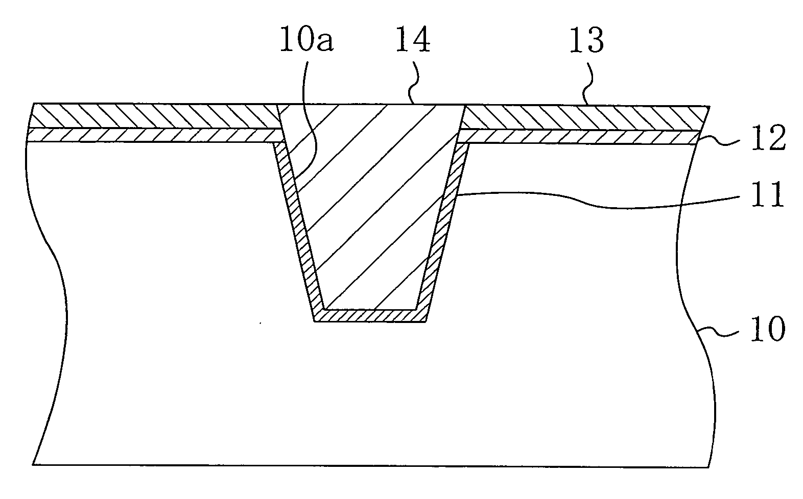
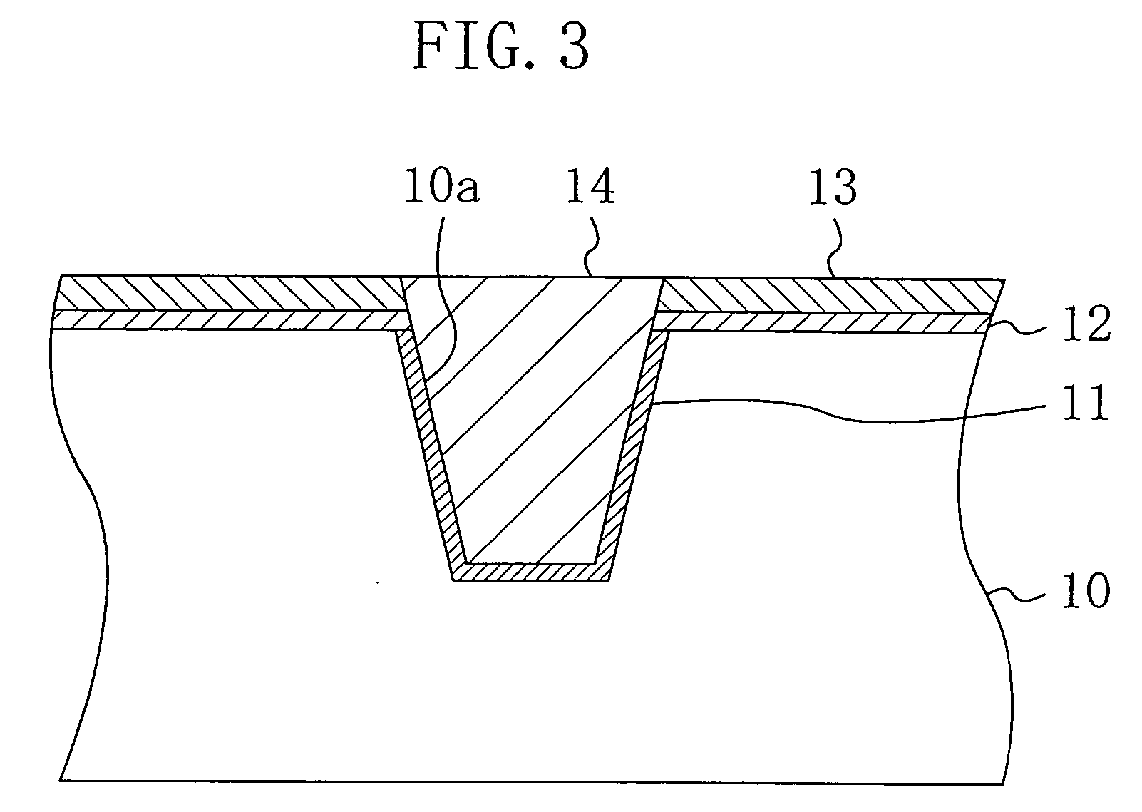
[0054]FIG. 3 shows a cross-sectional structure of a trench isolation region (STI) in the semiconductor device of the first embodiment.

[0055] As shown in FIG. 3, a semiconductor substrate 10 of silicon (Si) has a groove (trench) 10a which is 0.25 μm to 0.30 μm deep and 0.20 μm or less wide on top. For example, the trench 10a is filled with aluminum nitride, an insulating metal nitride. An STI 14 of aluminum nitride is thus formed in the upper part of the semiconductor substrate 10. Note that the above dimensions of the trench 10a are shown by way of example only and the dimensions of the trench 10a are not limited to the above values. The semiconductor substrate 10 is not limited to a silicon wafer. The semiconductor substrate 10 may be an SOI (silicon on insulator) substrate having an insulating laye...

second embodiment

[0074] Hereinafter, a semiconductor device and a manufacturing method thereof according to a second embodiment of the present invention will be described with reference to the drawings.

[0075]FIG. 9 shows a cross-sectional structure of a trench isolation region (STI) in the semiconductor device of the second embodiment. In FIG. 9, the same elements as those of FIG. 3 are denoted with the same reference numerals and characters, and description thereof will be omitted.

[0076] As shown in FIG. 9, an adhesive layer 15 of aluminum oxide (Al2O3) is formed between an STI 14 of aluminum nitride (AlN) and a sidewall oxide film 11 which is formed on the bottom and the wall surface of a trench 10a formed in the upper part of a semiconductor substrate 10. The adhesive layer 15 is about 5 nm thick and is formed in order to improve adhesion between the sidewall oxide film 11 and the STI 14.

[0077] The adhesive layer 15 is formed not only on the inner surface of the trench 10a but on the respectiv...

third embodiment

[0083] Hereinafter, a semiconductor device and a manufacturing method thereof according to a third embodiment of the present invention will be described with reference to the drawings.

[0084]FIG. 11 shows a cross-sectional structure of a trench isolation region (STI) in the semiconductor device of the third embodiment. In FIG. 11, the same elements as those of FIG. 3 are denoted with the same reference numerals and characters, and description thereof is omitted.

[0085] As shown in FIG. 11, an STI 14 of the third embodiment has a first filler 16 of aluminum nitride (AlN) and a second filler 17 of silicon oxide (SiO2) as fillers of a trench 10a. The first filler 16 is formed on the bottom and the wall surface of the trench 10a. The remaining portion of the trench 10a is filled with the second filler 17.

[0086] In the third embodiment, the trench 10a formed in the upper part of the semiconductor substrate 10 is not filled only with the first filler 16 of aluminum nitride but with both ...


PUM

PropertyMeasurementUnit
thermal conductivityaaaaaaaaaa
thicknessaaaaaaaaaa

Abstract

A semiconductor device has a semiconductor layer of silicon which has a plurality of element formation regions, and a trench isolation region for isolating the plurality of element formation regions from each other. The trench isolation region is formed by filling a trench formed in an upper part of the semiconductor layer with an insulating metal nitride. A thermal expansion coefficient of the insulating metal nitride is closer to that of silicon than a thermal expansion coefficient of silicon oxide is to that of silicon.

Description

CROSS REFERENCE TO RELATED APPLICATIONS [0001] This application claims priority under 35 U.S.C. §119 on Patent Application No. 2004-308695 filed in Japan on Oct. 22, 2004, the entire contents of which are hereby incorporated by reference. BACKGROUND OF THE INVENTION [0002] The present invention generally relates to a semiconductor device and a manufacturing method thereof. More particularly, the present invention relates to a semiconductor device having trench isolation for isolating a plurality of elements from each other, and a manufacturing method thereof. [0003] For higher integration of elements, shallow trench isolation (STI) technology has been mainly used as an element isolation technology for elements of 0.25 μm or less design rule. In this technology, shallow trench isolation (STI) is formed by forming grooves (trenches) of about 0.2 μm to about 0.3 μm deep in a main surface of a semiconductor substrate and filling the trenches with an insulating material. With recent impr...

Claims


Application Information

Patent Timeline
Patent Type & Authority Applications(United States)
IPC IPC(8): H01L29/00
CPCH01L21/76232
Inventor OKUNO, YASUTOSHI
Owner PANASONIC CORP
Why Eureka
Try Eureka