Semiconductor device including metal-insulator-metal capacitor arrangement
a technology of metal-insulator metal and capacitor, which is applied in the direction of semiconductor devices, semiconductor/solid-state device details, capacitors, etc., can solve the problems of difficult or impossible to obtain the conformity between the capacitances of mim capacitors, and achieve the effect of suppressing the production of parasitic capacitan
- Summary
- Abstract
- Description
- Claims
- Application Information
AI Technical Summary
Benefits of technology
Problems solved by technology
Method used
Image
Examples
first embodiment
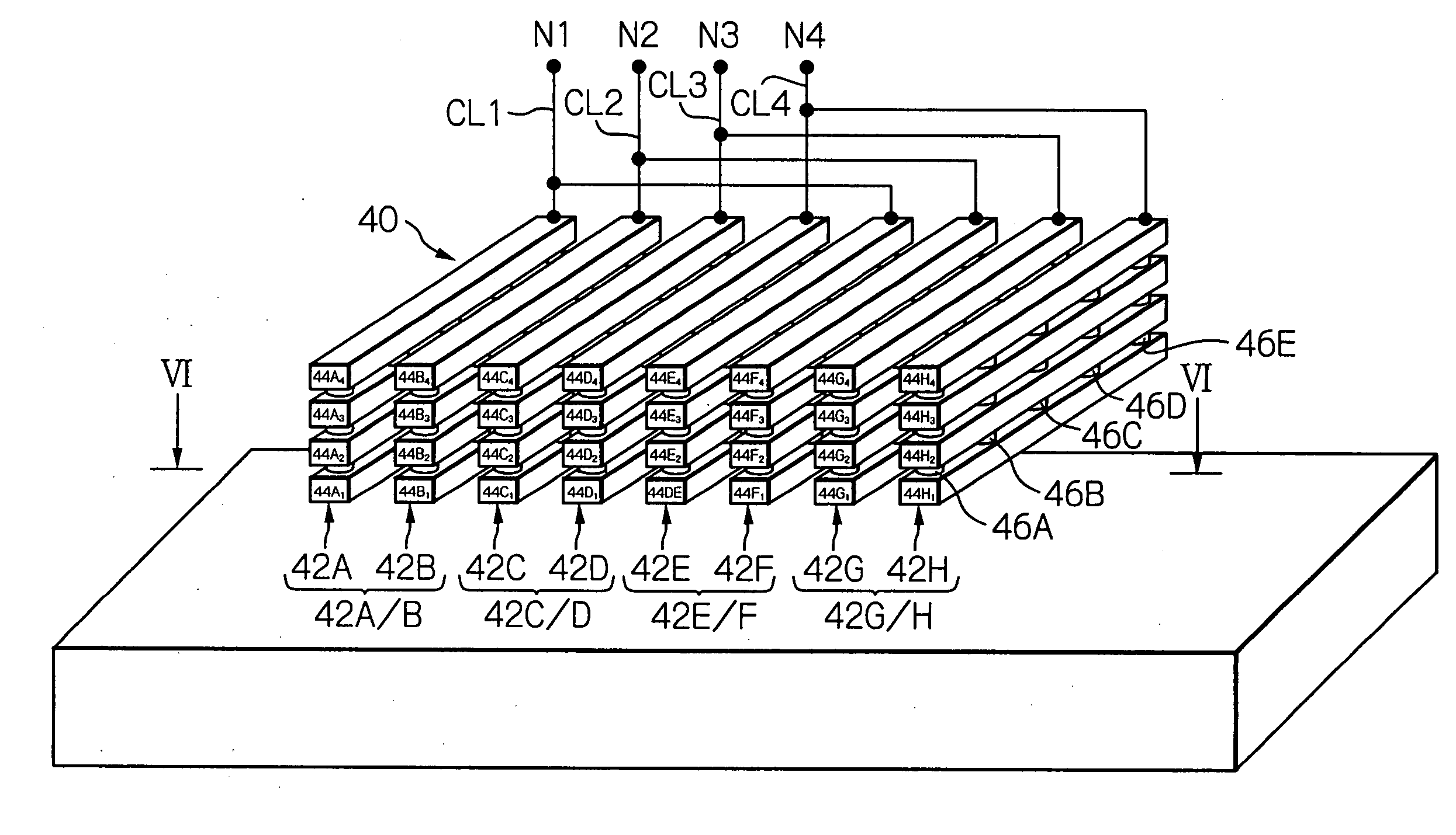
[0080]FIGS. 5, 6, 7 and 8 show a first embodiment of a semiconductor device including an MIM capacitor arrangement according to the present invention.
[0081] In FIGS. 5, 7 and 8, reference SS indicates a semiconductor substrate which defines one of chip areas on a silicon wafer, and only a part of the semiconductor substrate SS is illustrated. Although not shown in FIGS. 5 and 6, after a semiconductor device is produced in the semiconductor substrate SS by processing the silicon wafer, using various well-known methods, a multi-layered wiring construction MWC (FIGS. 7 and 8) is formed over the semiconductor substrate SS.
[0082] As shown in FIGS. 7 and 8, the multi-layered wiring construction MWC includes a lowermost wiring layer LWL formed over the semiconductor substrate SS, an intermediate wiring layer IWL formed over the lowermost wiring layer LWL, and a global wiring layer GWL formed over the intermediate wiring Layer IWL. In this embodiment, the intermediate wiring layer IWL inc...
second embodiment
[0116]FIGS. 9 and 10 show a second embodiment of an semiconductor device including an MIM capacitor arrangement according to the present invention. Note, FIG. 9 shows a cross-section of the MIM capacitor arrangement taken along the IX-IX line of FIG. 10, and FIG. 10 shows a cross-section of the MIM capacitor arrangement taken along the IX-IX line of FIG. 10 is a cross-sectional view taken along the X-X line of FIG. 9.
[0117] In FIG. 10, reference SS′ indicates a semiconductor substrate which defines one of chip areas on a silicon wafer, and only a part of the semiconductor substrate SS is illustrated. Although not shown in FIGS. 9 and 10, after a semiconductor device is produced in the semiconductor substrate SS by processing the silicon wafer, using various well-known methods, a multi-layered wiring construction MWC′ is formed over the semiconductor substrate SS′.
[0118] As shown in FIG. 10, the multi-layered wiring construction MWC′ includes a lowermost wiring layer LWL′ formed ov...
PUM
 Abstract
Description
Claims
Application Information
 - R&D
- Intellectual Property
- Life Sciences
- Materials
- Tech Scout
- Unparalleled Data Quality
- Higher Quality Content
- 60% Fewer Hallucinations
Browse by: Latest US Patents, China's latest patents, Technical Efficacy Thesaurus, Application Domain, Technology Topic, Popular Technical Reports.
© 2025 PatSnap. All rights reserved.Legal|Privacy policy|Modern Slavery Act Transparency Statement|Sitemap|About US| Contact US: help@patsnap.com


