Layer fill for homogenous technology processing

a technology of homogenous technology and layer filling, applied in semiconductor devices, semiconductor/solid-state device details, electrical devices, etc., can solve the problems of unused or wasted surface area of semiconductor devices, non-uniform feature size across wafers, and unpredictable performance and characteristics of semiconductor devices b>100/b>, so as to promote a uniform etching and cmp environment for the gate material layer, the effect of improving the dof of lithography processes

Inactive Publication Date: 2006-05-04
INFINEON TECH AG
View PDF11 Cites 4 Cited by
  • Summary
  • Abstract
  • Description
  • Claims
  • Application Information

AI Technical Summary

Benefits of technology

[0021] Advantages of embodiments of the present invention include providing a novel fill structure in a gate material layer simulating functional gate shapes, promoting a uniform etch and CMP environment for the gate material layer. A plurality of functional transistors having uniform resistance and other electrical parameters are produced by embodiments of the present invention. Because the planarity of the gate material layer is improved, the DOF of lithography processes is improved for subsequently deposited material layers of the semiconductor device. Advantageously, the novel fill structures may be used to form spare transistors, in some embodiments.

Problems solved by technology

A problem that occurs in some semiconductor device designs is non-uniformity of feature sizes across a wafer.
Gates G for transistors 108a and 108b having different dimensions is undesirable in some semiconductor designs, because this results in the transistor gates G in region 104 having different electrical properties and characteristics than the transistor gates G in region 106.
This also produces a semiconductor device 100 having unpredictable performance and characteristics.
However, this prior art approach results in unused or wasted surface area of the semiconductor device 100.
The fill structure 120 is not homogeneous enough to achieve a high yield in advanced technologies.

Method used


Image

  • Layer fill for homogenous technology processing
  • Layer fill for homogenous technology processing
  • Layer fill for homogenous technology processing

Examples


Embodiment Construction

[0034] The making and using of the presently preferred embodiments are discussed in detail below. It should be appreciated, however, that the present invention provides many applicable inventive concepts that can be embodied in a wide variety of specific contexts. The specific embodiments discussed are merely illustrative of specific ways to make and use the invention, and do not limit the scope of the invention.

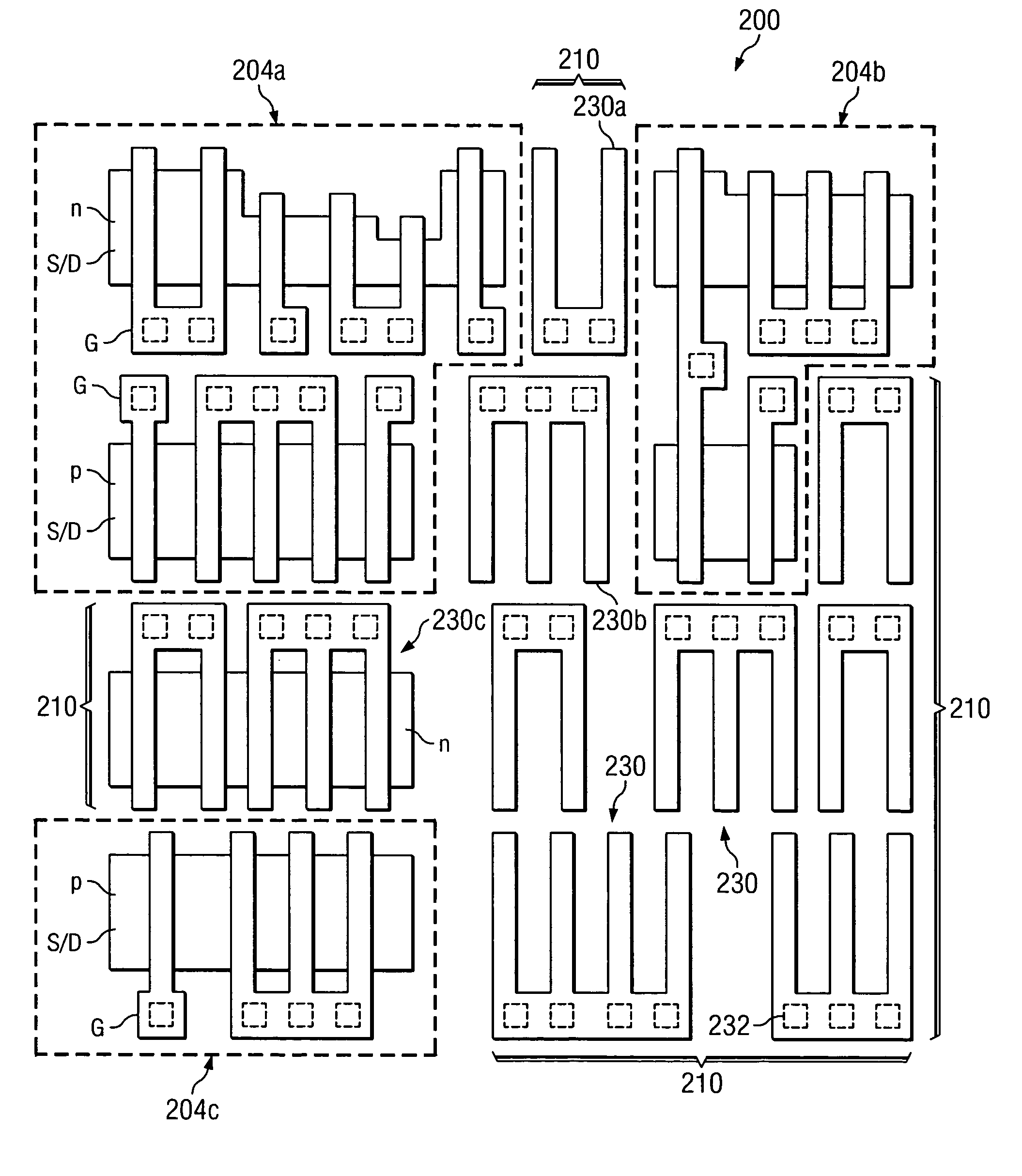
[0035]FIG. 3 shows a top view of a novel layer fill structure in accordance with an embodiment of the present invention implemented in the semiconductor device design shown in FIG. 2, e.g., having a plurality of blocks of functional transistor gates separated by wide spaces. Like numerals are used as reference numbers for the various elements shown as were used in FIGS. 1 and 2.

[0036] Regions 204a, 204b, and 204c have a plurality of functional gates G formed therein. The functional gates G comprise one or more fingers of polysilicon and other gate materials that extend ove...


PUM


Abstract

Spare transistors are formed in regions of a semiconductor device where functional transistors are not formed, providing uniformity in etch and polishing processes, and resulting in transistors with more uniform parameters on the semiconductor device. The spare transistors may not be electrically connected to other components on the device, or alternatively, the spare transistors may be connected to other components for use as spare transistors, for example. The gates of the spare transistors provide a homogeneous gate material layer, resulting in improved etch, polishing, and lithography processes for the semiconductor device.

Description

TECHNICAL FIELD [0001] The present invention relates generally to the design and manufacture of semiconductor devices, and more particularly to a layer fill for improved uniformity of semiconductor device features formed by chemical mechanical polish and etch processes. BACKGROUND [0002] Semiconductor devices are used in a variety of electronic applications, such as computers, cellular phones, personal computing devices, and many other applications. Home, industrial, and automotive devices that in the past comprised only mechanical components now have electronic parts that require semiconductor devices, for example. [0003] Semiconductor devices are manufactured by depositing many different types of material layers over a semiconductor workpiece or wafer, and patterning the various material layers using lithography. There may be a plurality of transistors, memory devices, switches, conductive lines, diodes, capacitors, logic circuits, and other electronic components formed on a singl...

Claims


Application Information

Patent Timeline
Patent Type & Authority Applications(United States)
IPC IPC(8): H01L21/82H01L29/76
CPCH01L21/31053H01L21/32134H01L21/32136H01L27/0207H01L29/4238
Inventor POECHMUELLER, PETER
Owner INFINEON TECH AG
Why Eureka
Try Eureka