Lateral double diffused MOS transistors

a technology of mos and mos, which is applied in the direction of semiconductor devices, electrical equipment, semiconductor/solid-state device details, etc., can solve the problems reducing and shrinking the geometry, so as to improve the mechanical structure and improve the mechanical integrity of comb electrodes. , the effect of increasing the likelihood of mechanical failure of comb electrode geometries

Inactive Publication Date: 2006-05-04
BELL SEMICON LLC
View PDF2 Cites 14 Cited by
  • Summary
  • Abstract
  • Description
  • Claims
  • Application Information

AI Technical Summary

Benefits of technology

[0006] We have developed an improved mechanical structure for MOS transistor devices with elongated runners. It recognizes that shrinking the geometry increases the likelihood of mechanical failure of comb electrode geometries. The mechanical integrity of the comb electrode is improved by interconnecting the electrode fingers in a cross-connected grid. In one embodiment, the transistor device is interconnected with gate fingers on a lower metaliization level, typically the first level metal, with the drain interconnected at a higher metal level. That allows the drain fingers to be cross-connected with vertical separation between drain and gate combs. The drain comb, with cross-connections, may be formed at the second level, but preferably skips a level to, for example, the third level, to increase the separation and potential capacitive coupling between the drain and gate. To further reduce capacitive coupling, an interlevel ground plane may be used. The ground plane may be formed in the skipped level.

Problems solved by technology

It recognizes that shrinking the geometry increases the likelihood of mechanical failure of comb electrode geometries.

Method used


Image

  • Lateral double diffused MOS transistors
  • Lateral double diffused MOS transistors
  • Lateral double diffused MOS transistors

Examples


Embodiment Construction

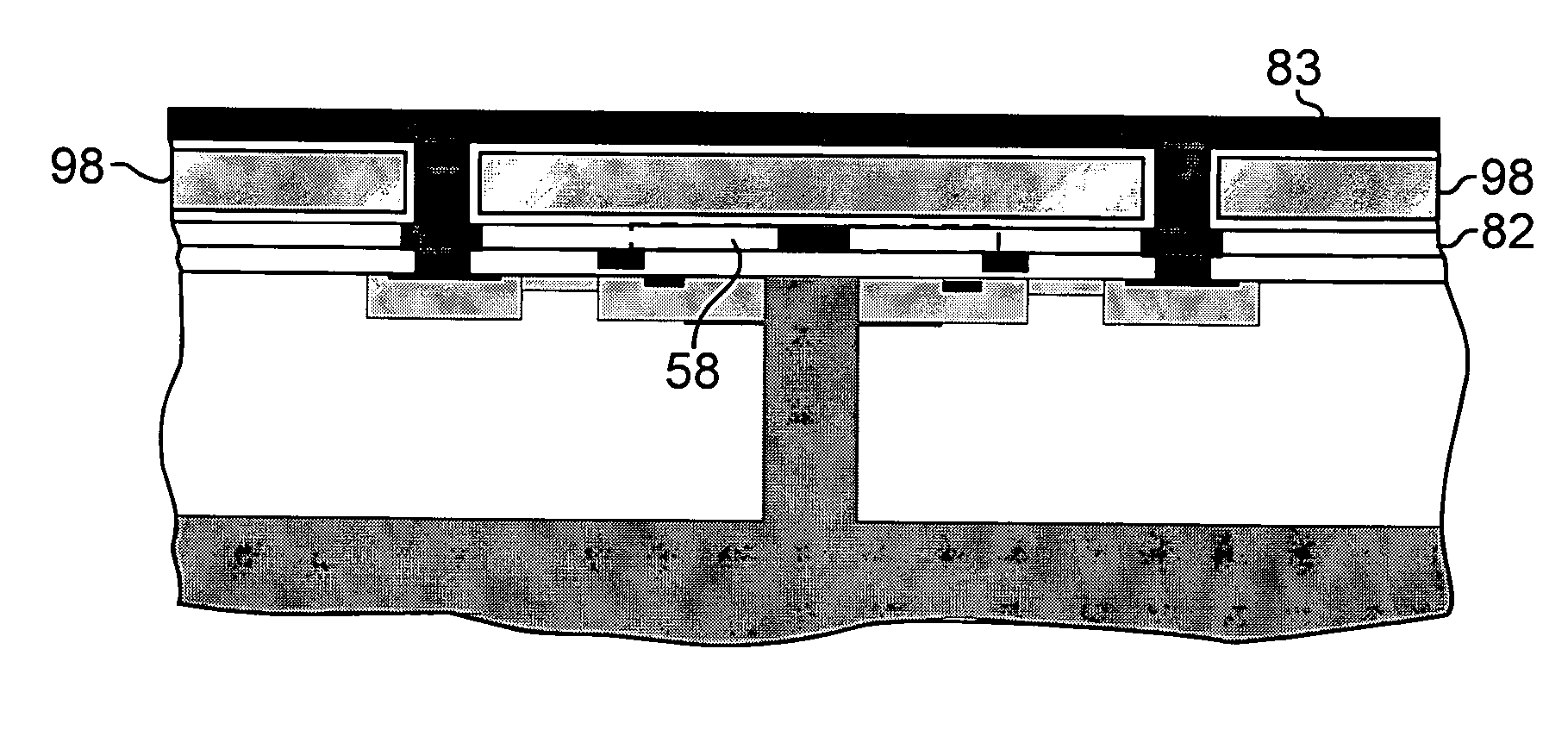
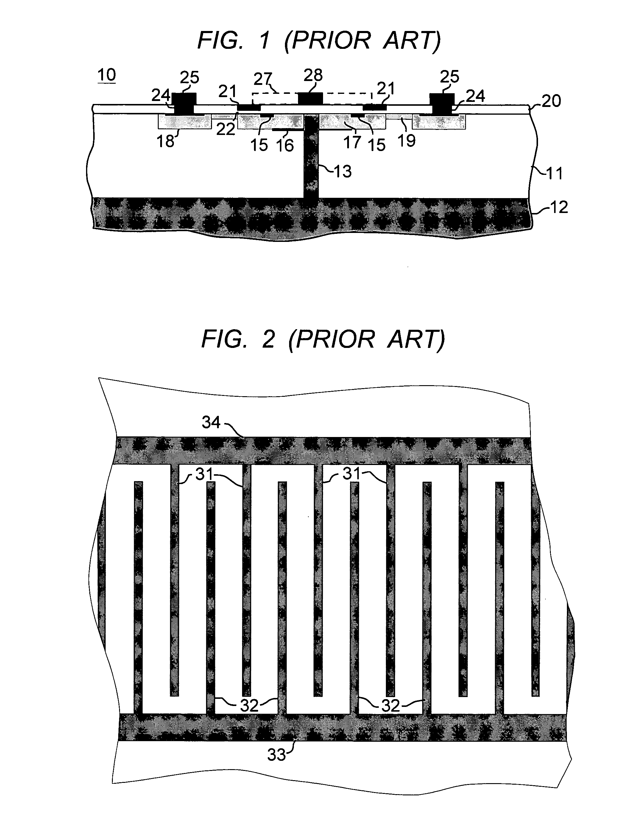
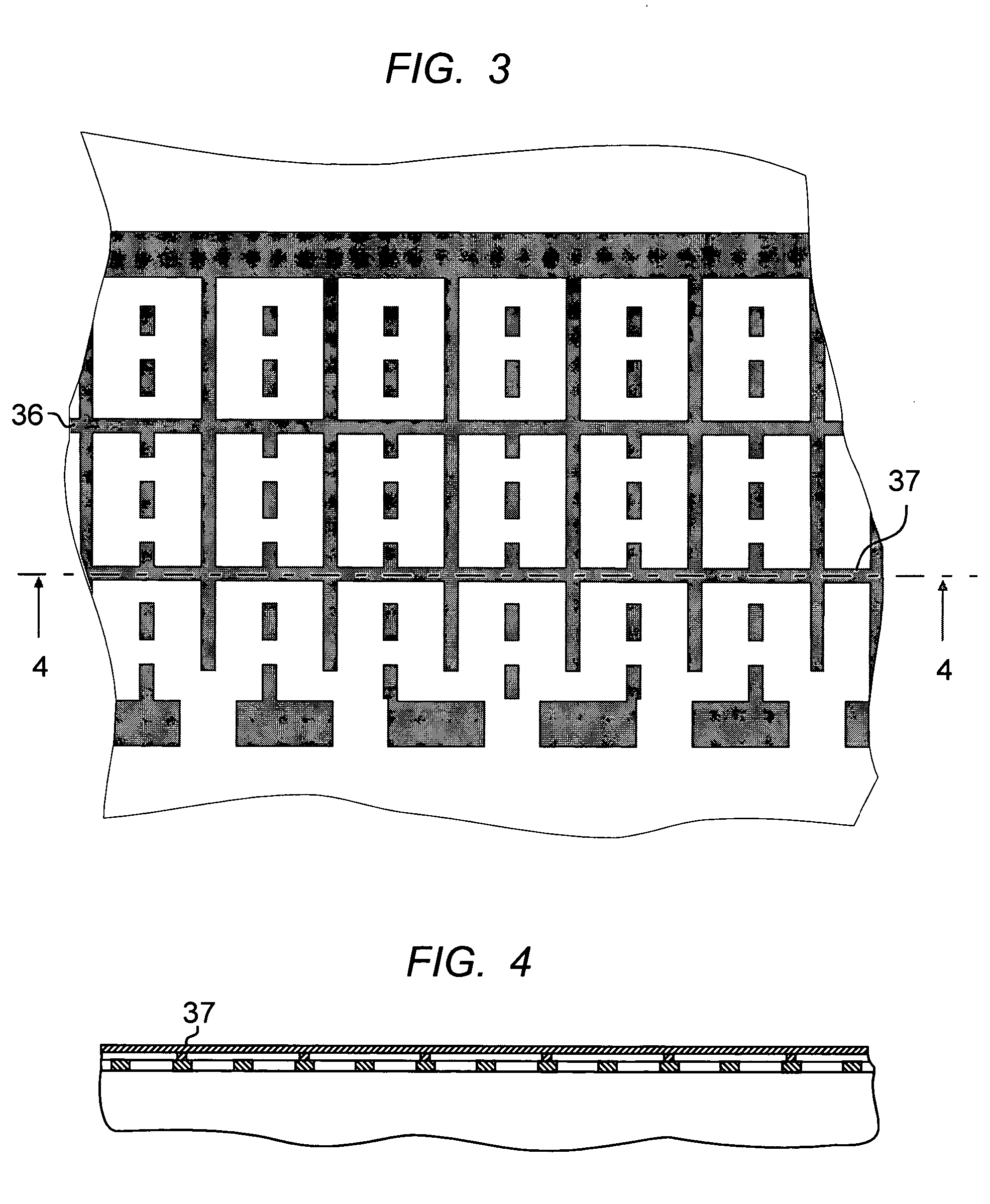
[0021] In state of the art RF LDMOS power devices the surface electrodes are typically drain and gate, with the gate interconnections formed on the first level. That device format will be used in the following description to illustrate the invention. However, it should be understood that the invention may apply to other device configurations.

[0022] Referring to FIG. 1, an RF LDMOS device is shown generally at 10, with p-type epitaxial substrate 11 and p+ buried region 12. The buried region in this device configuration comprises the source and is formed by well-known implant and epitaxial growth techniques. The buried region is accessed electrically via source sinker 13. It is noted that the elements in the figures are not drawn to scale. The transistor source comprises n+ implant 15, with deep p+ implant 16 and surface p-type implant 17 forming the drift region. The drain implant is shown at 18, and the lightly doped drain extension (LDD) at 19. The basic device structure just desc...


PUM


Abstract

The specification describes an improved mechanical electrode structure for MOS transistor devices with elongated runners. It recognizes that shrinking the geometry increases the likelihood of mechanical failure of comb electrode geometries. The mechanical integrity of a comb electrode is improved by interconnecting the electrode fingers in a cross-connected grid. In one embodiment, the transistor device is interconnected with gate fingers on a lower metaliization level, typically the first level metal, with the drain interconnected at a higher metal level. That allows the drain fingers to be cross-connected with a vertical separation between drain and gate comb electrodes. The cross-connect members may be further stabilized by adding beam extensions to the cross-connect members. The beam extensions may be anchored in an interlevel dielectric layer for additional support.

Description

FIELD OF THE INVENTION [0001] The field of the invention is design and fabrication of lateral double diffused MOS (LDMOS) transistors. BACKGROUND OF THE INVENTION [0002] Double diffused (DMOS) transistors are used widely in both RF analog and mixed-signal integrated circuits (ICs), and in dielectrically isolated ICs for power and high voltage applications. These devices are produced in both vertical and lateral configurations. In the lateral configuration (LDMOS) the power handling property of the device is enhanced by extending the active portion of the device along the x-y plane of the substrate. In a typical implementation the active region meanders in a serpentine pattern to increase the length to width ratio of the overall device. [0003] The surface electrode configurations for these devices are substantially elongated, and may be relatively complex. In a common power device structure, the elongated gate and drain elements are formed in a comb configuration with the combs facin...

Claims


Application Information

Patent Timeline
Patent Type & Authority Applications(United States)
IPC IPC(8): H01L23/62
CPCH01L23/4824H01L29/402H01L29/4175H01L29/41758H01L29/41775H01L29/4238H01L29/7835H01L2924/0002H01L2924/00
Inventor DESKO, JOHN C.FRATTI, ROGER A.RYAN, VIVIAN
Owner BELL SEMICON LLC
Why Eureka
Try Eureka