Probe card interposer

a probe card and interposer technology, applied in the field of modular probe cards, can solve the problems of difficult to precisely control the contact the ics circuit design becomes more complicated, and the shifting of the tips of the interposer is a problem, so as to achieve accurate electrical contact and good mechanical strength

Inactive Publication Date: 2006-05-04
CHIPMOS TECH INC
View PDF5 Cites 37 Cited by
  • Summary
  • Abstract
  • Description
  • Claims
  • Application Information

AI Technical Summary

Benefits of technology

[0006] A main purpose of the present invention is to provide a probe card interposer which comprises a substrate with a plurality of conductive bumps. Each conductive bump further includes a dielectric core and a plurality of contact wires. One ends of the contact wires are bonded to the bonding pads of the substrate adjacent to the corresponding dielectric cores. The other ends of the contact wires are suspended and extend toward the centers of the corresponding dielectric cores such that the contact wires are elastically supported by the corresponding dielectric cores. Therefore, the interposer can possesses the capability of elastic and electrical contact with the probe head and the multi-layer PCB to assemble a modularized probe head to resolve the common issues of an interposer for poor coplanarity leading to electrically open and excessive stresses leading to breaking of the electrical contacts. Moreover, since the dielectric bumps are elastic and the contact wires are supported by the dielectric cores, the contact wires manufactured by MEMS or wire bonding can achieve accurate electrical contact with good mechanical strengths.

Problems solved by technology

However, since the circuit design of ICs becomes more complicated, only a probe card with high density of probes can fully test the electrical functions of the ICs and precisely screen out all the failed ICs.
When the interposer is installed between a PCB and a probe head, the tips of the interconnection elements of the interposer are difficult to control to precisely contact with fine pitch pads on the PCB or the probe head to make electrical connections.
Accordingly, the shifting of the tips of the interconnection elements is a problem due to lack of firm support.
However, during the assembly of a probe card, the first probes and the second probes of the interposer are vulnerable to bending or breaking.

Method used


Image

  • Probe card interposer
  • Probe card interposer
  • Probe card interposer

Examples


first embodiment

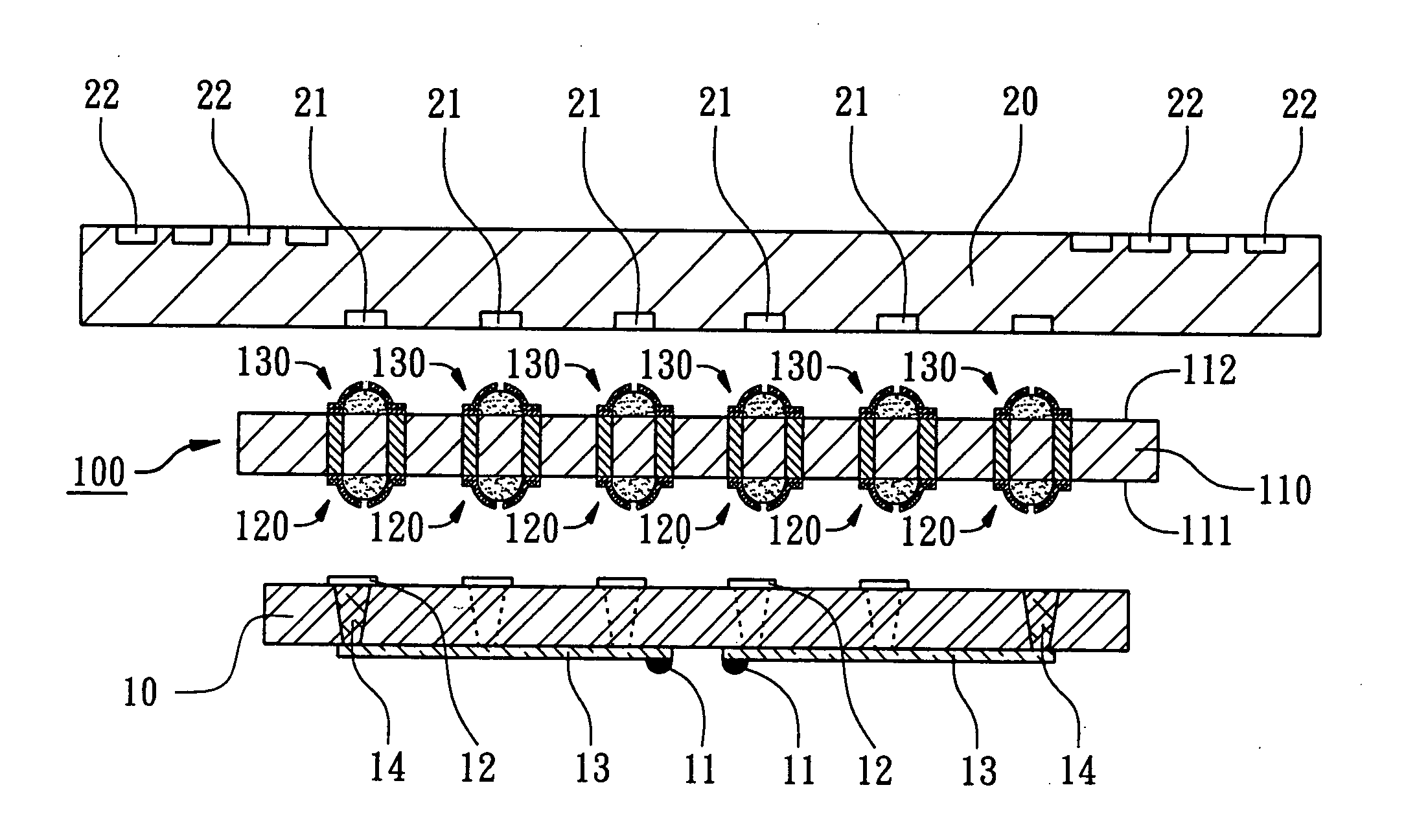
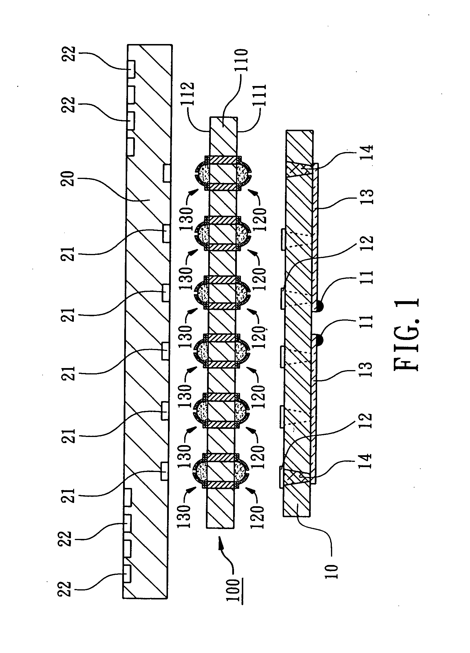
[0018] The first embodiment according to present invention, as shown in FIG. 1, a probe card interposer 100 is configured for disposing between a probe head 10 and a multi-layer PCB 20 to assemble a modularized probe card. The probe head 10 is made of Si wafers, ceramic substrates, or glass substrates. The probe head 10 has a plurality of probing components 11 such as probes or bumps for probing the bonding pads of ICs, where the probing components 11 are electrically connected to the contact pads 12 on the other surface of the probe head 10 through dedicated circuits 13 and vias 14. The multi-layer PCB 20 has a plurality of contact pads 21 and a plurality of pogo pads 22, where the contact pads 21 are electrically connected to the contact pads 12, and the pogo pads 22 are configured to connect the corresponding pogo pins on the test head of a tester (not shown in the drawings).

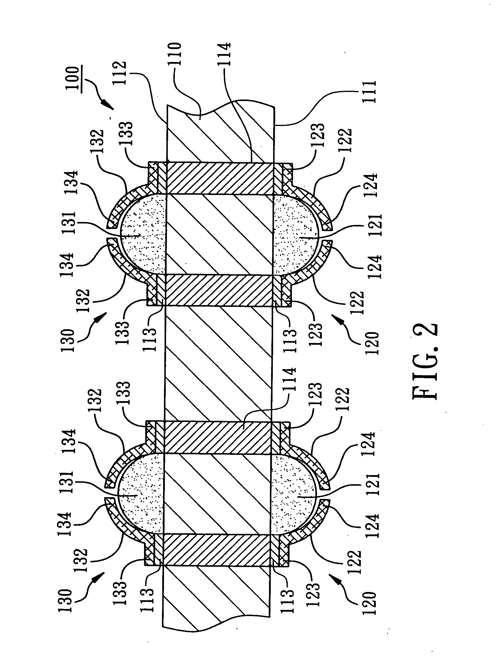
[0019] As shown in FIG. 2, the interposer 100 includes a substrate 110 and a plurality of first conductive...

second embodiment

[0023] According to the present invention, as shown in FIG. 3, a modularized probe card comprises a probe head 30, a multi-layer PCB 40 and an interposer 200 disposed between the probe head 30 and the multi-layer PCB 40. A plurality of probes 31 are disposed on one surface of the probe head 30 and a plurality of contact pads 32 on the other surface of the probe head 30. A plurality of contact pads 41 are disposed on one surface of the multi-layer PCB 40 and are electrically connected to the contact pads 32 of the probe head 30 by the interposer 200. The interposer 200 and the probe head 30 can be joined together to be a one-piece component by disposing and curing the underfill material 50 between the interposer 200 and the probe head 30 to ensure good electrical contacts between both. A fixture is used to fix the one-piece component including the interposer 200 and the probe head 30 to the multi-layer PCB 40 to reduce the alignment errors.

[0024] As shown in FIG. 4, the interposer 20...

third embodiment

[0026] According to the present invention, as shown in FIG. 6 and FIG. 7, a probe card interposer 300 includes a substrate 310, a plurality of first conductive bumps 320 and a plurality of second conductive bumps 330. The substrate 310 has a first surface 311 and a second surface 312. The substrate includes a plurality of bonding pads 313 on the first surface 311, a plurality of second bonding pads 314 on the second surface 312, and a plurality of conductive posts 315. The first bonding pads 313 are electrically connected to the second bonding pads 314 through the conductive posts 315. The first conductive bumps 320 are disposed on the first bonding pads 313, and the second conductive bumps 330 on the second bonding pads 314. The second conductive bumps 330 are vertically aligned with the first conductive bumps 320. Each first conductive bump 320 includes a plurality of first contact wires 321 formed by wire bonding. Each first conductive wire 321 has two first fixed end 322 and a f...


PUM


Abstract

A probe card interposer includes a substrate with a plurality of conductive bumps disposed on first surface of the substrate. Each conductive bump comprises a dielectric core and a plurality of conductive leads. The suspended ends of the conductive wires extend toward the centers of the corresponding dielectric cores and are elastically supported by the corresponding dielectric cores. Therefore, the interposer can be installed between a probe head and a multi-layer PCB to make good electrical contacts to the probe head through the conductive bumps. In the embodiment, a plurality of symmetric conductive bumps are disposed on second surface of the substrate and are electrically connected to the conductive bumps on first surface of the substrate through vias or conductive posts. The conductive bumps can electrically contact the multi-layer PCB.

Description

FIELD OF THE INVENTION [0001] The present invention relates to a modularized probe card, and more particularly, to an interposer for modularized probe cards. BACKGROUND OF THE INVENTION [0002] During the fabrication of integrated circuits (IC), either in wafer form or package form, testing is required to ensure ICs in good electrical functions. However, since the circuit design of ICs becomes more complicated, only a probe card with high density of probes can fully test the electrical functions of the ICs and precisely screen out all the failed ICs. Moreover, a probe card with capable circuit designs and good probe mechanical and electrical characteristics will provide accurate testing results without underkill or overkill. [0003] An IC tester comprises a test head for installing a probe card which serves as an electrical contact medium between a tester and Dies Uunder Test (DUT). Under the consideration of lower manufacturing costs, a probe card is modularized and comprises a multi...

Claims


Application Information

Patent Timeline
Patent Type & Authority Applications(United States)
IPC IPC(8): H01L23/02
CPCG01R1/0416G01R31/2889H05K3/326H05K3/4092H05K2201/0397H05K2201/09909H05K2201/10378
Inventor LIU, AN-HONGWANG, YEONG-HERLEE, YAO-JUNG
Owner CHIPMOS TECH INC
Why Eureka
Try Eureka