
Stacking system and method

a technology of integrated circuits and stacking chips, applied in the direction of printed circuit manufacturing, printed circuit non-printed electric components association, printed circuit aspects, etc., can solve the problems of not providing a technology for stacking chip scale packages, significant expense, and require topologies of added cost and complexity, and achieve reasonable cost production, easy to understand and manage

Inactive Publication Date: 2006-05-04
ENTORIAN TECH
View PDF23 Cites 26 Cited by
  • Summary
  • Abstract
  • Description
  • Claims
  • Application Information

AI Technical Summary

Benefits of technology

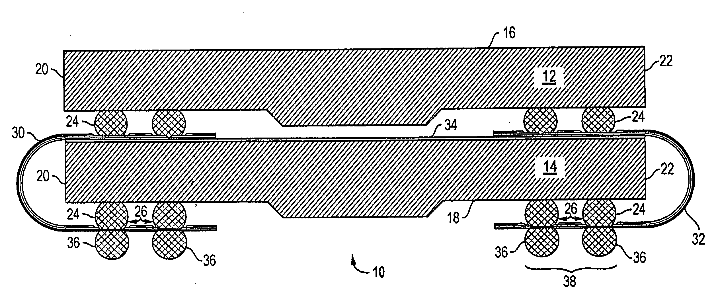
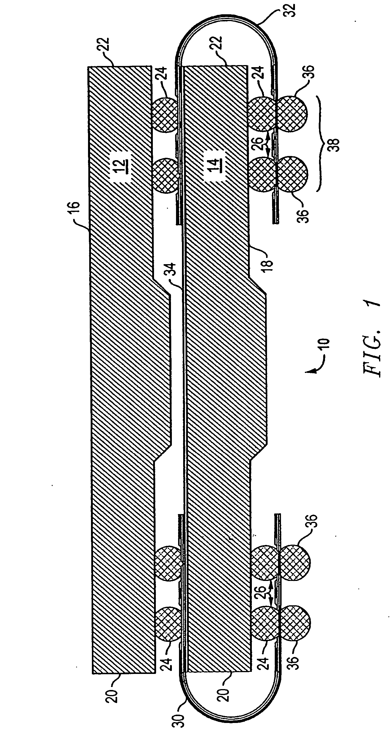
[0017] In a two-high CSP stack or module devised in accordance with a preferred embodiment of the present invention, two CSPs are stacked, with one CSP disposed above the other. The two CSPs are connected with a pair of flex circuits. Each of the pair of flex circuits is partially wrapped about a respective opposite lateral edge of the lower CSP of the module. The flex circuit pair connects the upper and lower CSPs and provides a thermal and electrical path connection path between the module and an application environment such as a printed wiring board (PWB).

Problems solved by technology

Those S-CSP specifications describe, however, stacking multiple die within a single chip scale package and do not provide a technology for stacking chip scale packages.
Stacking integrated circuits within a single package requires specialized technology that includes reformulation of package internals and significant expense with possible supply chain vulnerabilities.
Such techniques provide alternatives, but require topologies of added cost and complexity.
The previous known methods for stacking CSPs apparently have various deficiencies including complex structural arrangements and thermal or high frequency performance issues.
During such reliability evaluations, CSP devices often exhibit temperature cycle performance issues.
The issues associated with temp cycle performance in single CSPs will likely arise in those prior art CSP stacking solutions where the stack is offset from the PWB or application platform by only the height of the lower CSP ball grid array.
Prior art solutions to CSP stacking do not, however, address thermal gradient minimization in disclosed constructions.

Method used


Image

  • Stacking system and method
  • Stacking system and method
  • Stacking system and method

Examples


Embodiment Construction

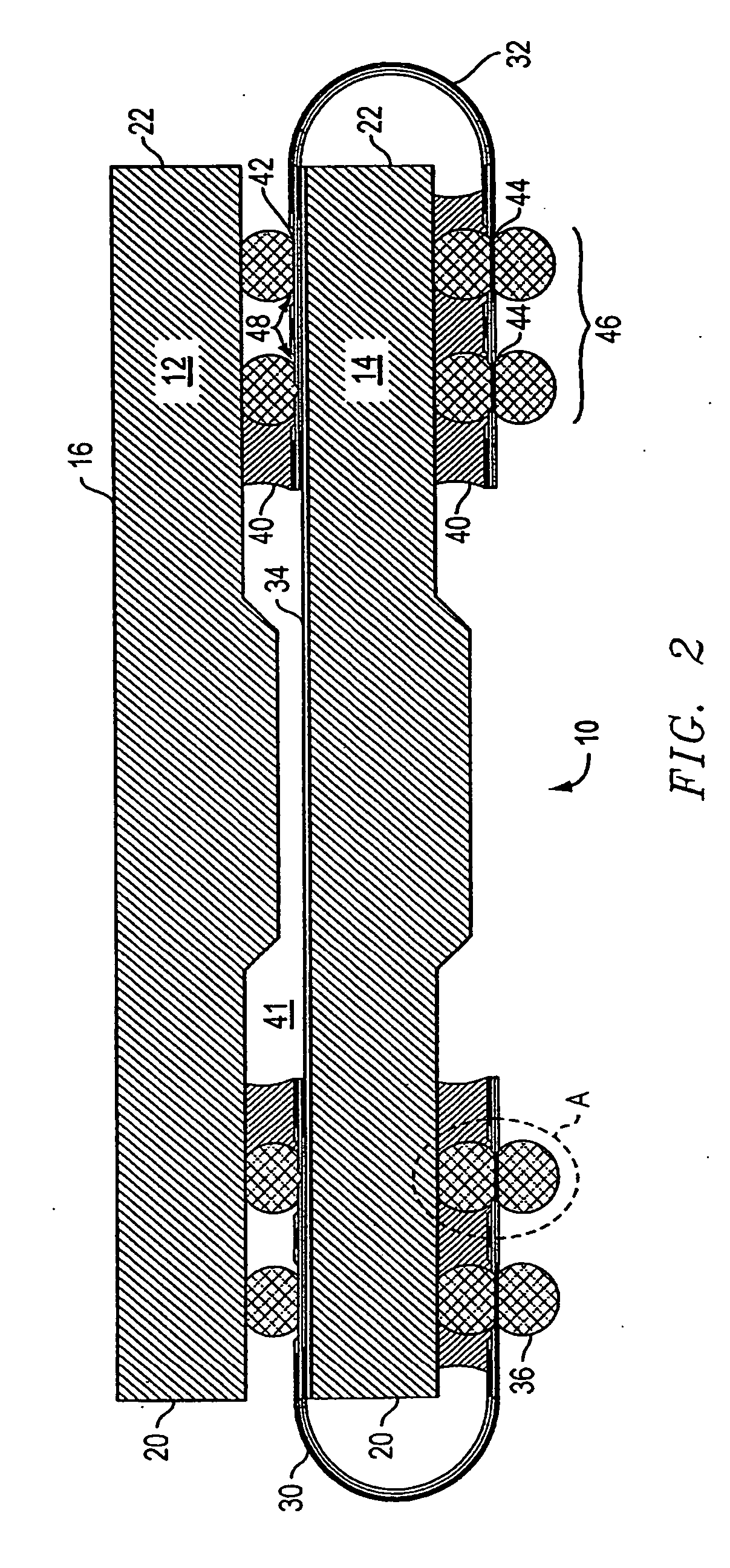
[0041]FIG. 1 is an elevation view of module 10 devised in accordance with a preferred embodiment of the present invention. Module 10 is comprised of upper CSP 12 and lower CSP 14. Each of CSPs 12 and 14 have an upper surface 16 and a lower surface 18 and opposite lateral sides 20 and 22.

[0042] The invention is used with CSP packages of a variety of types and configurations such as, for example, those that are die-sized, as well those that are near chip-scale as well as the variety of ball grid array packages known in the art. Collectively, these will be known herein as chip scale packaged integrated circuits (CSPs) and preferred embodiments will be described in terms of CSPs, but the particular configurations used in the explanatory figures are not, however, to be construed as limiting. For example, the elevation views of FIGS. 1 and 2 are depicted with CSPs of a particular profile known to those in the art, but it should be understood that the figures are exemplary only. Later fig...


PUM


Abstract

The present invention stacks integrated circuits into modules that conserve board surface area. In a two-high stack or module devised in accordance with a preferred embodiment of the present invention, a pair of integrated circuits is stacked, with one integrated circuit above the other. The two integrated circuits are connected with a pair of flexible circuit structures. Each of the pair of flexible circuit structures is partially wrapped about a respective opposite lateral edge of the lower integrated circuit of the module. The flex circuit pair connects the upper and lower integrated circuits and provides a thermal and electrical path connection path between the module and an application environment such as a printed wiring board (PWB). The present invention may be employed to advantage in numerous configurations and combinations of integrated circuits in modules provided for high-density memories or high capacity computing.

Description

RELATED APPLICATIONS [0001] This application is a continuation of U.S. application Ser. No. 10 / 400,309 filed Mar. 27, 2003, which is a continuation of U.S. application Ser. No. 10 / 005,581, filed Oct. 26, 2001, now issued as U.S. Pat. No. 6,576,992, each of which is hereby incorporated by reference for all purposes.TECHNICAL FIELD [0002] The present invention relates to aggregating integrated circuits and, in particular, to stacking integrated circuits in chip-scale packages. BACKGROUND OF THE INVENTION [0003] A variety of techniques are used to stack packaged integrated circuits. Some methods require special packages, while other techniques stack conventional packages. In some stacks, the leads of the packaged integrated circuits are used to create a stack, while in other systems, added structures such as rails provide all or part of the interconnection between packages. In still other techniques, flexible conductors with certain characteristics are used to selectively interconnect ...

Claims


Application Information

Patent Timeline
IPC IPC(8): H01L23/48H01L23/31H01L23/498H01L23/538H01L25/065H01L25/10H05K1/14H05K1/18H05K3/36
CPCH01L23/3114H01L23/49816H01L23/49827H01L23/4985H01L23/5387H01L25/0657H01L25/105H01L2224/16237H01L2225/06517H01L2225/06541H01L2225/06579H01L2225/06586H01L2924/19041H01L2924/3011H05K1/141H05K1/147H05K1/189H05K3/363H05K2201/056H05K2201/10689H05K2201/10734H01L2924/01087H01L2225/107
Inventor CADY, JAMES W.WILDER, JAMESROPER, DAVID L.WEHRLY, JAMES DOUGLAS JR.DOWDEN, JULIANBUCHLE, JEFF
Owner ENTORIAN TECH
Learn More