Ceramic antenna module and methods of manufacture thereof

a ceramic dielectric and antenna module technology, applied in the direction of resonant antennas, substantially flat resonant elements, particular array feeding systems, etc., can solve the problems of physical size and occupie a larger footprint, and achieve the effect of reducing internal reflection and improving radiation efficiency

Active Publication Date: 2006-05-04
DE ROCHEMONT L PIERRE
View PDF69 Cites 506 Cited by
  • Summary
  • Abstract
  • Description
  • Claims
  • Application Information

AI Technical Summary

Benefits of technology

[0015] The present invention provides circuit modules that contain at least one antenna element or at least one ultra-low loss transmission line in an interconnect structure supplying RF electromagnetic energy to an antenna element formed by embedding discrete wire or other type conductors within a pure amorphous silica, alumina, titania, or other suitable ceramic dielectric. The present invention also provides a method of constructing a ceramic dielectric meta-material that has a high effective value of real permittivity but which minimizes reflective losses, through the use of a host dielectric (organic or ceramic) having a relative permittivity substantially less than the embedded ceramic dielectric inclusions used to form the dielectric meta-material, and further allows the physical lengths of the antenna element(s), formed either with discrete wire conductors or patterned film, to be minimized without adversely impacting radiation efficiency. The meta-material structure may additionally provide frequency band filtering functions that would normally be provided by other components typically found in an RF front-end, and methods to construct the same. In a preferred embodiment of the invention the host dielectric is selected to have a minimal loss tangent to maximize the efficiency of the circuit module.

Problems solved by technology

Physical size is another critical issue in mobile platform design.
This forces many module manufacturers to backside mount the semiconductor die and connect it to the interconnect structure through wire bonds located on the die's periphery, which then occupies a larger footprint.

Method used


Image

  • Ceramic antenna module and methods of manufacture thereof
  • Ceramic antenna module and methods of manufacture thereof
  • Ceramic antenna module and methods of manufacture thereof

Examples


Embodiment Construction

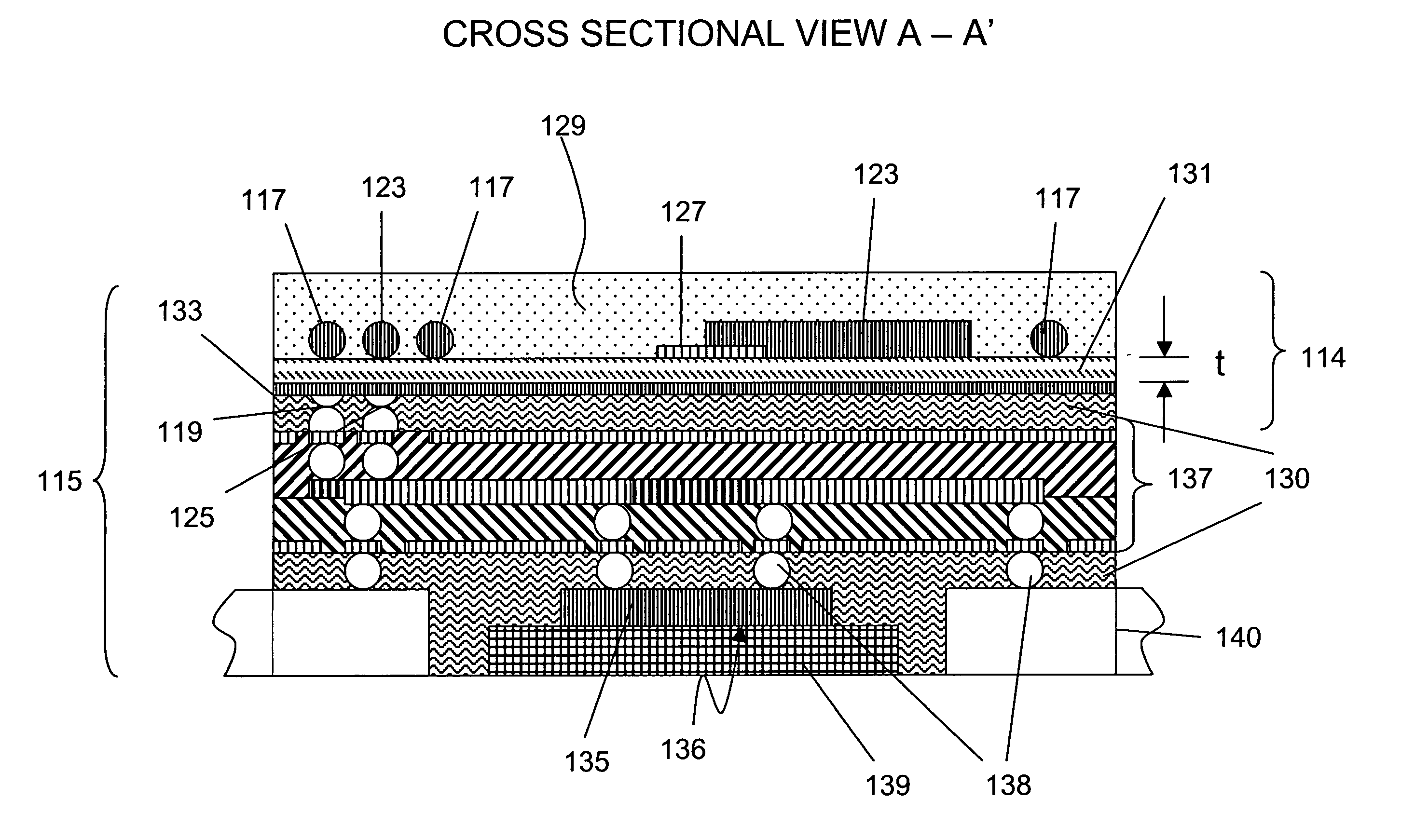
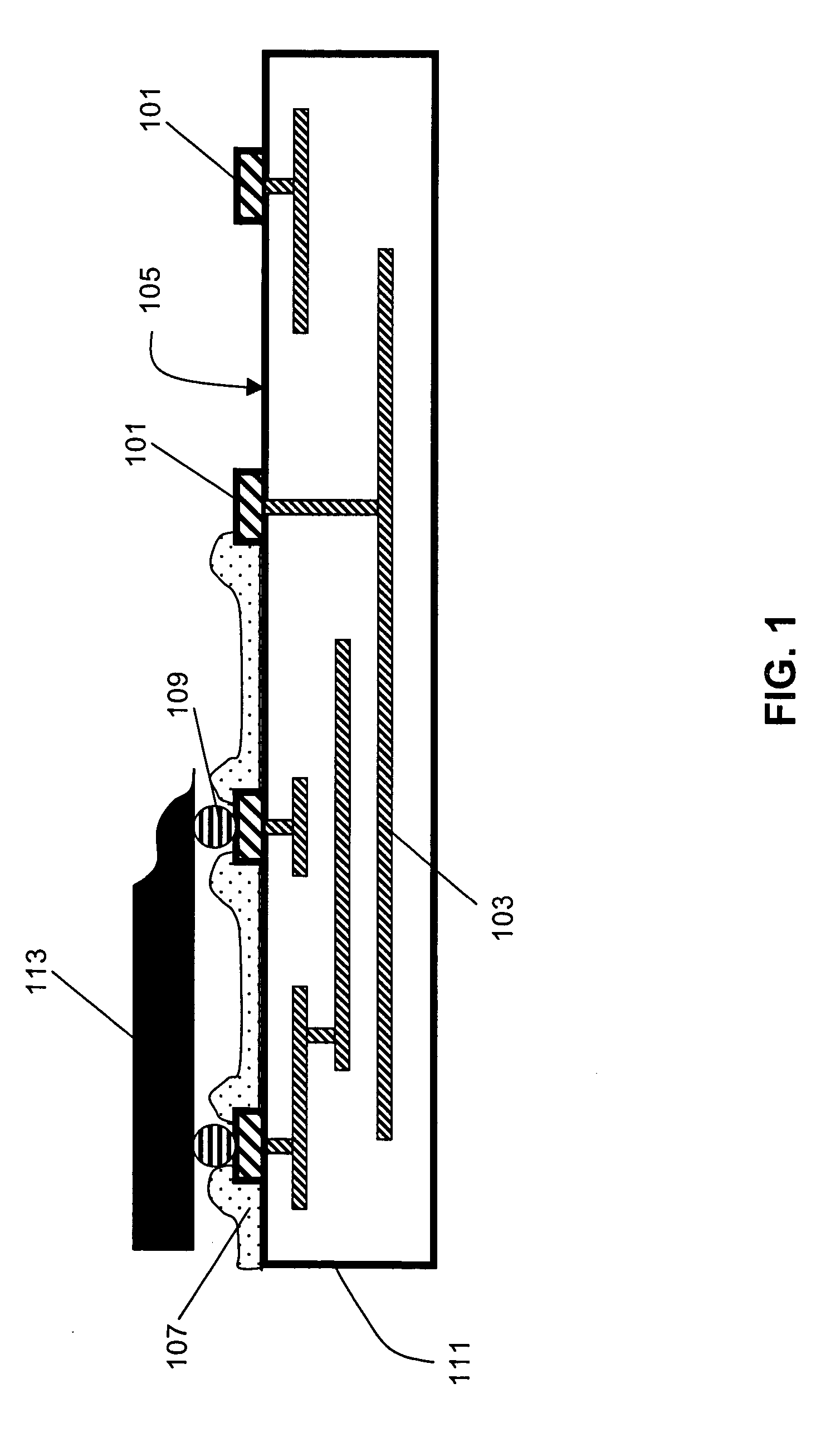
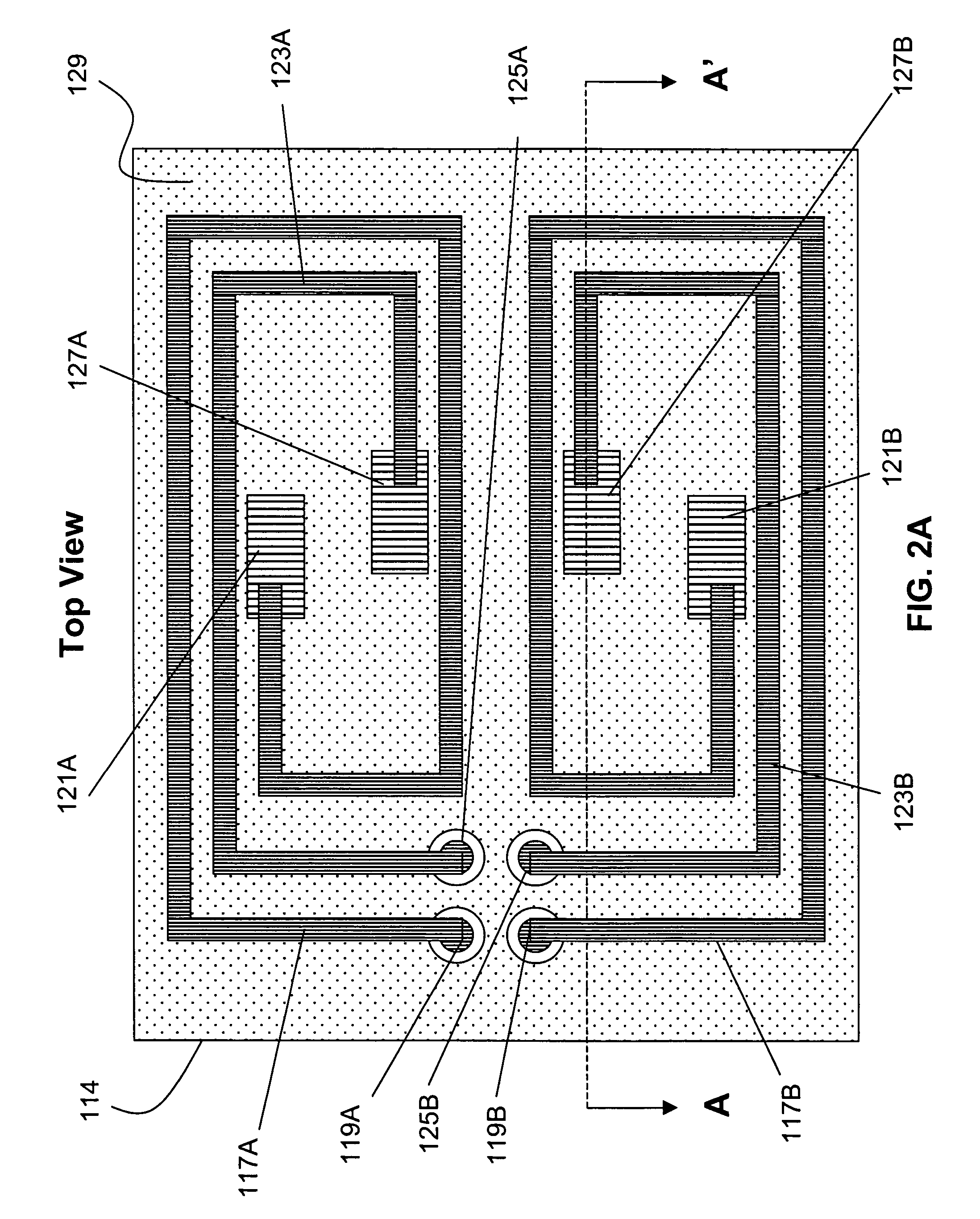
[0078] Reference is now made to FIGS. 2A thru 4 and FIGS. 6 thru 11, which illustrate preferred embodiments of various aspects of a wireless circuit module 115 in accordance with the present invention, and FIGS. 5A-5J and 12A,B, which illustrate the processing steps used to create the circuit module. Circuit module 115 includes, in its most complete embodiment, an antenna module 114, which is in turn comprised of a composite ceramic dielectric body, at least one electrically conductive element, a low attenuation interconnect structure, and a metallization layer adjacent the composite dielectric body and including a ground plane structure and at least one contact pad. References to “discrete wires” are intended to denote pre-fabricated, conducting wire bodies that are geometrically uniform along their lengths and, when comprised of metal, which contain significantly higher metallurgical purity and geometric uniformity than is possible for traces made from conductive pastes or pattern...


PUM

PropertyMeasurementUnit
grain sizeaaaaaaaaaa
smoothnessaaaaaaaaaa

Abstract

Circuit modules and methods of construction thereof that contain composite meta-material dielectric bodies that have high effective values of real permittivity but which minimize reflective losses, through the use of host dielectric (organic or ceramic), materials having relative permittivities substantially less than ceramic dielectric inclusions embedded therein. The composite meta-material bodies permit reductions in physical lengths of electrically conducting elements such as antenna element(s) without adversely impacting radiation efficiency. The meta-material structure may additionally provide frequency band filtering functions that would normally be provided by other components typically found in an RF front-end.

Description

CROSS-REFERENCE TO RELATED APPLICATIONS [0001] This application claims the benefit of priority to U.S. Provisional Patent Application Nos. 60 / 615,174 filed 1 Oct. 2004, and 60 / 716,306 filed 12 Sep. 2005, both of which are entitled “Ceramic Antenna Module and Method of Manufacture”, and contents of which are incorporated herein by reference as if set forth in their entirety.FIELD OF THE INVENTION [0002] The present invention relates generally to the construction of ceramic dielectric meta-material components that have high effective values of real permittivity but minimal body losses, and, more particularly, to small form factor wireless circuit modules operating in the radio frequency (RF) spectrum that contain at least one antenna element or at least one ultra-low loss transmission line. BACKGROUND OF THE INVENTION [0003] As used in the descriptions that follow, the term “meta-materials” refers to materials that possess unique macroscopic properties due to finer scale repetition or...

Claims


Application Information

Patent Timeline
Patent Type & Authority Applications(United States)
IPC IPC(8): H01Q1/38
CPCH01L2223/6677H01Q1/362H01Q1/38H01Q7/00H01Q9/0407H01Q15/0086H01Q21/0025H01L2924/0002H01Q15/0046H01Q15/006H01Q9/16H01L2924/00H01Q5/307
Inventor DE ROCHEMONT, L. PIERRE
Owner DE ROCHEMONT L PIERRE
Why Eureka
Try Eureka